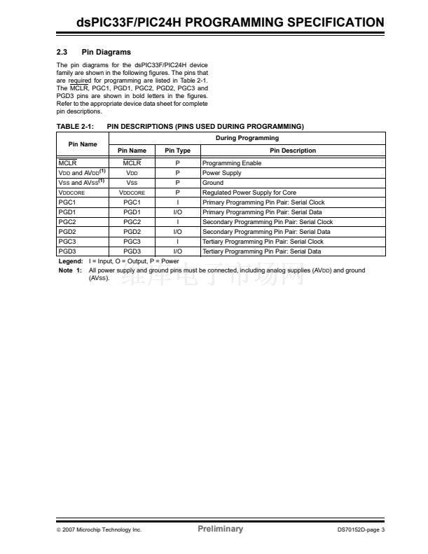
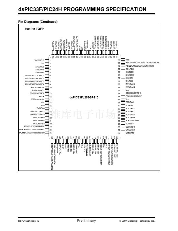
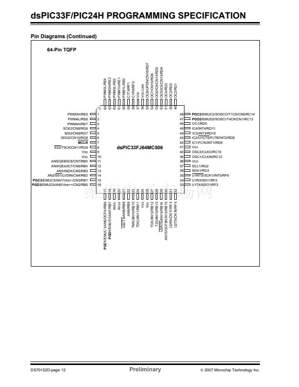
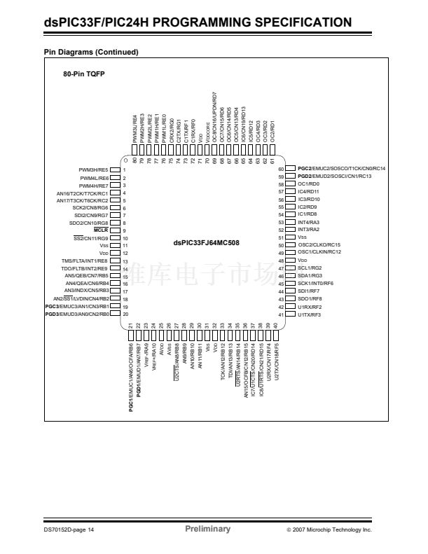
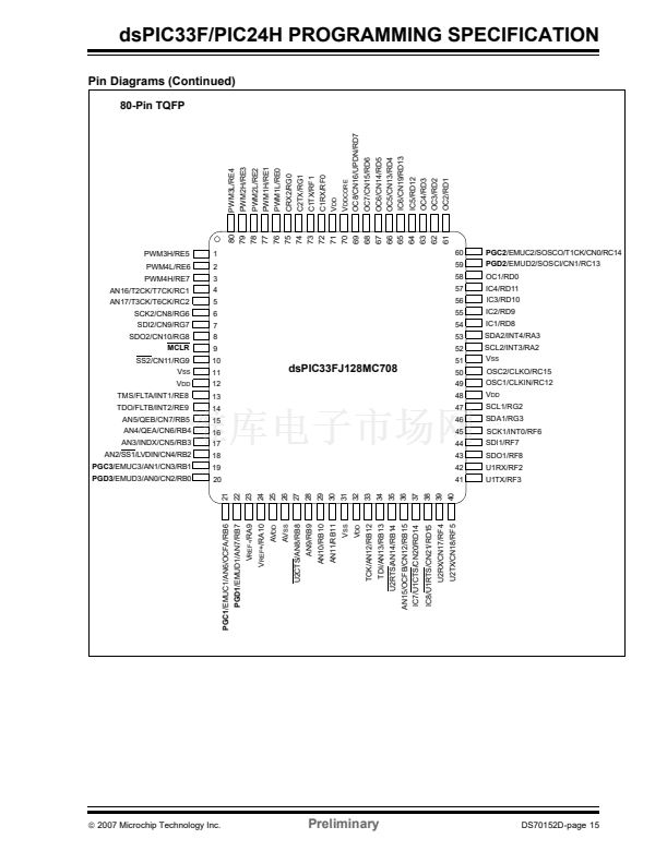
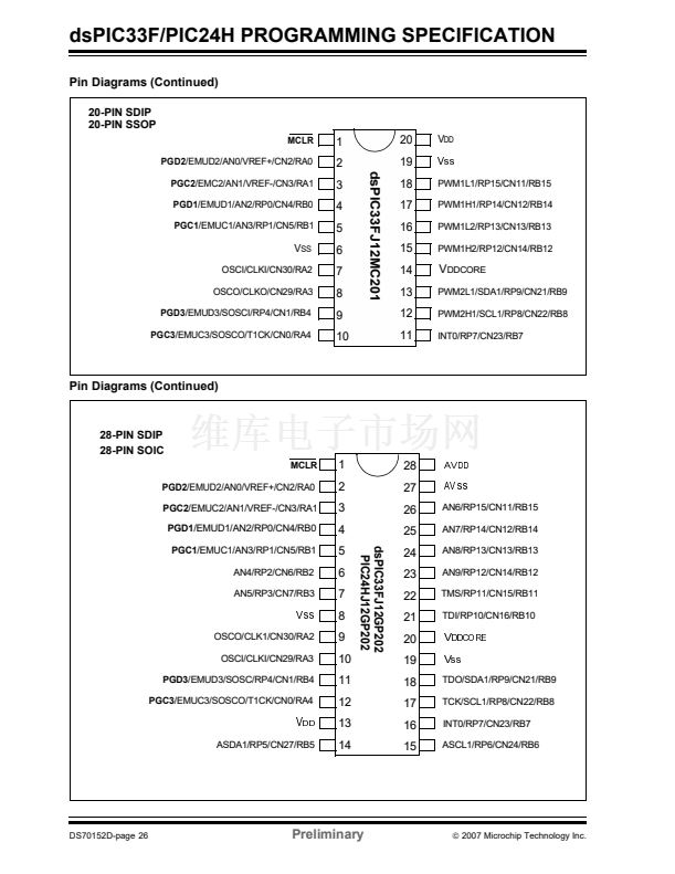
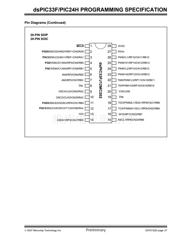
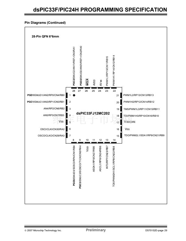
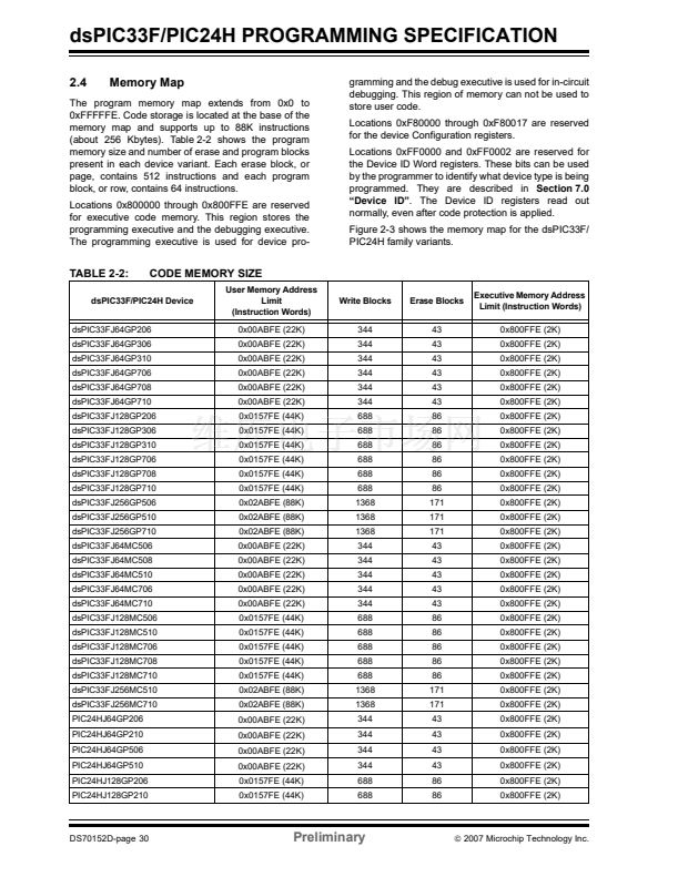
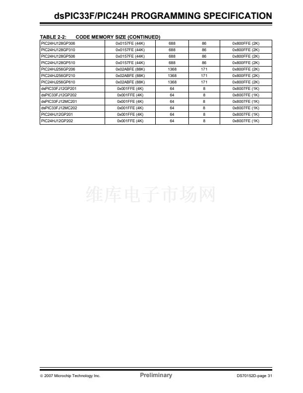
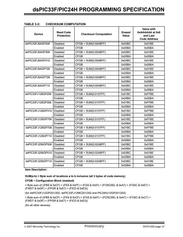
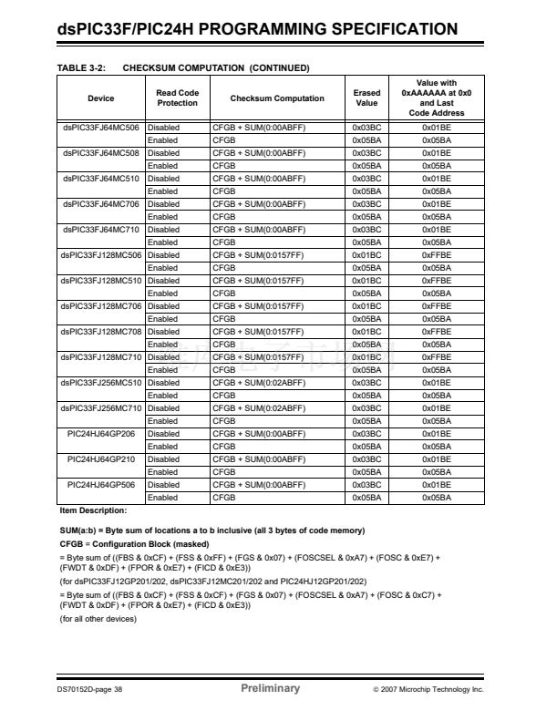
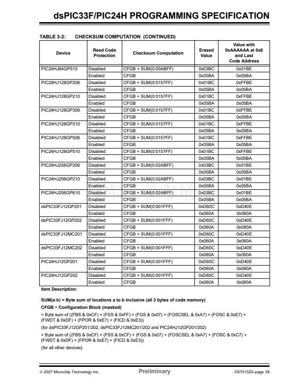
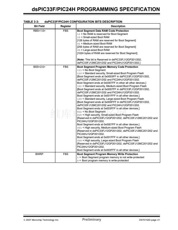
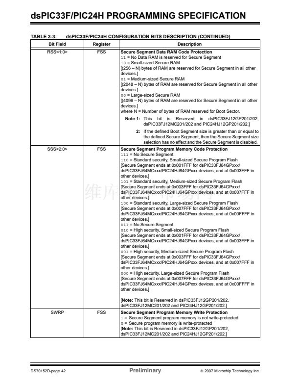
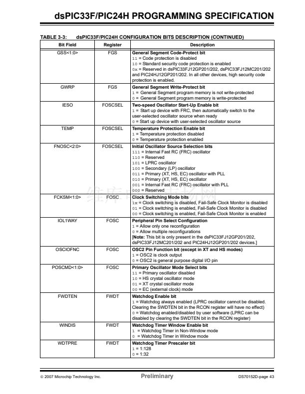
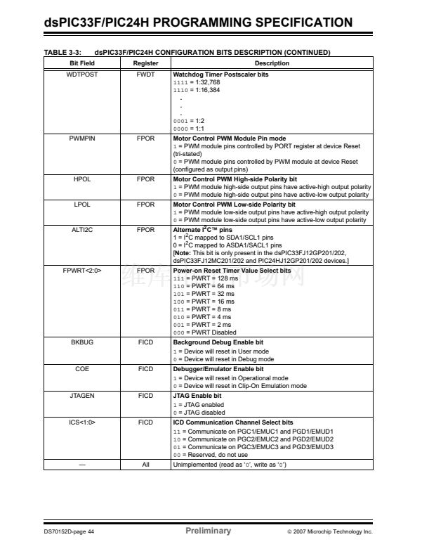
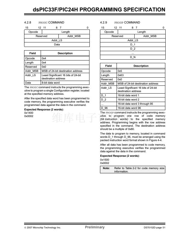
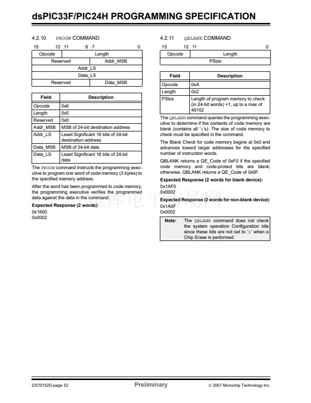
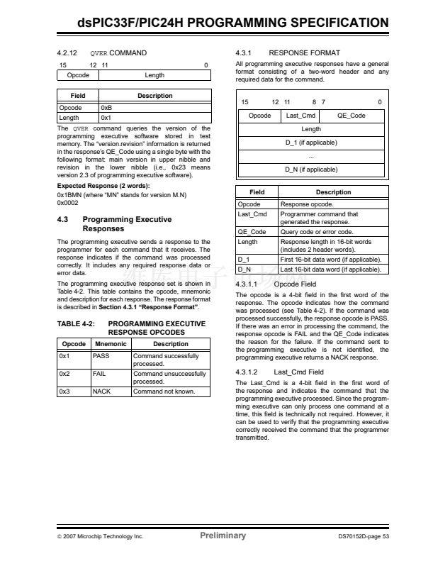
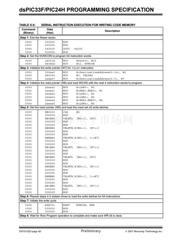
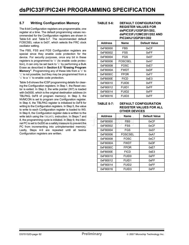
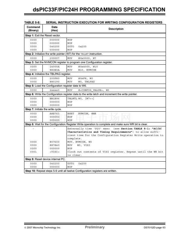
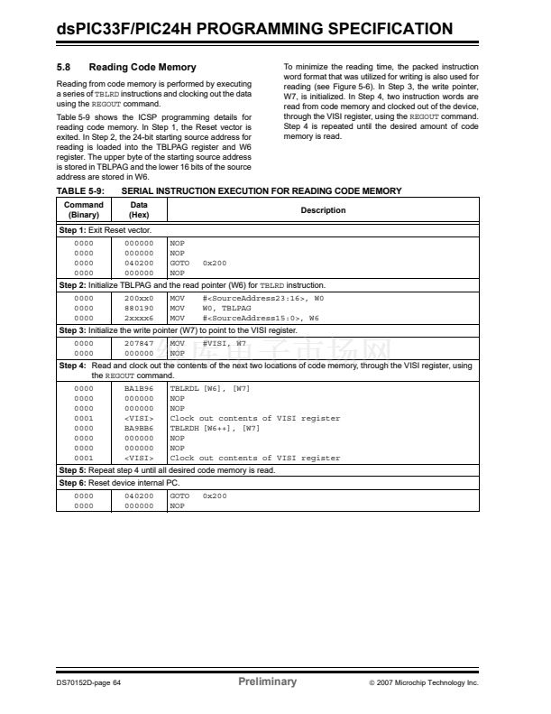
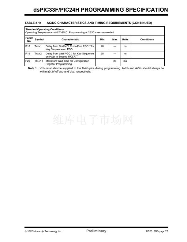
dsPIC33F/PIC24H PROGRAMMING SPECIFICATION
5.10
Verify Code Memory and
Configuration Word
5.11
Reading the Application ID Word
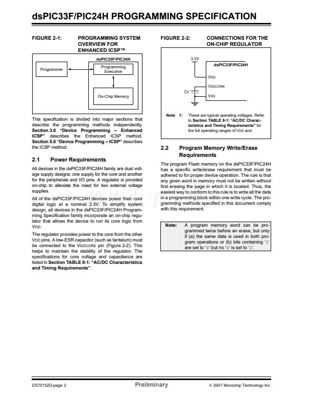
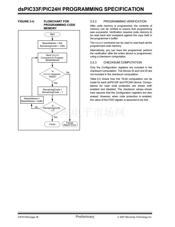
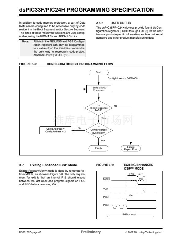
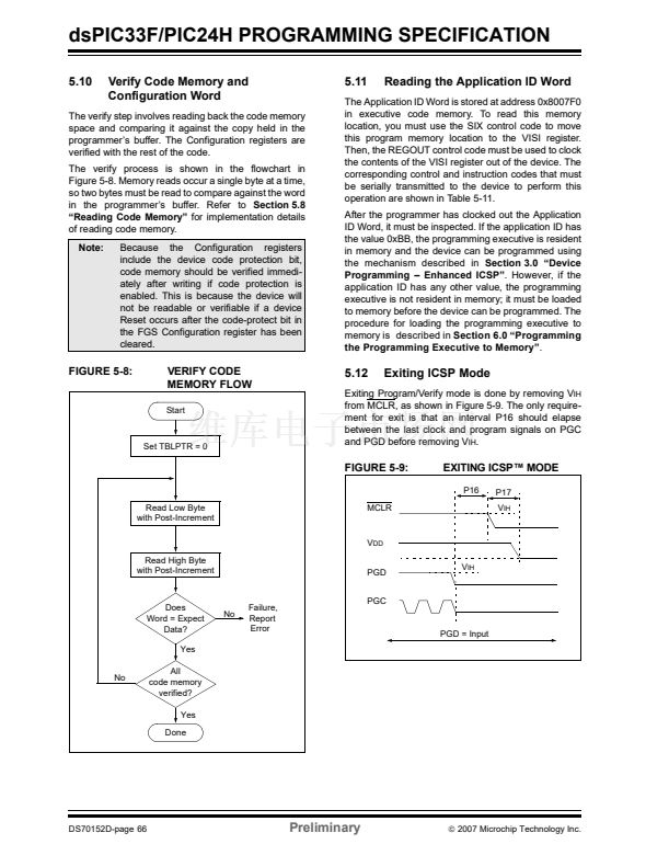
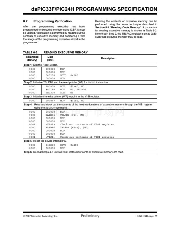
The verify step involves reading back the code memory
space and comparing it against the copy held in the
programmer鈥檚 buffer. The Configuration registers are
verified with the rest of the code.
The verify process is shown in the flowchart in
Figure 5-8. Memory reads occur a single byte at a time,
so two bytes must be read to compare against the word
in the programmer鈥檚 buffer. Refer to
Section 5.8
鈥淩eading Code Memory鈥?/span>
for implementation details
of reading code memory.
Note:
Because the Configuration registers
include the device code protection bit,
code memory should be verified immedi-
ately after writing if code protection is
enabled. This is because the device will
not be readable or verifiable if a device
Reset occurs after the code-protect bit in
the FGS Configuration register has been
cleared.
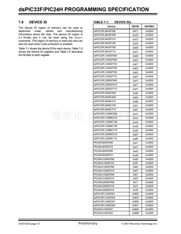
The Application ID Word is stored at address 0x8007F0
in executive code memory. To read this memory
location, you must use the SIX control code to move
this program memory location to the VISI register.
Then, the REGOUT control code must be used to clock
the contents of the VISI register out of the device. The
corresponding control and instruction codes that must
be serially transmitted to the device to perform this
operation are shown in Table 5-11.
After the programmer has clocked out the Application
ID Word, it must be inspected. If the application ID has
the value 0xBB, the programming executive is resident
in memory and the device can be programmed using
the mechanism described in
Section 3.0 鈥淒evice
Programming 鈥?Enhanced ICSP鈥?
However, if the
application ID has any other value, the programming
executive is not resident in memory; it must be loaded
to memory before the device can be programmed. The
procedure for loading the programming executive to
memory is described in
Section 6.0 鈥淧rogramming
the Programming Executive to Memory鈥?
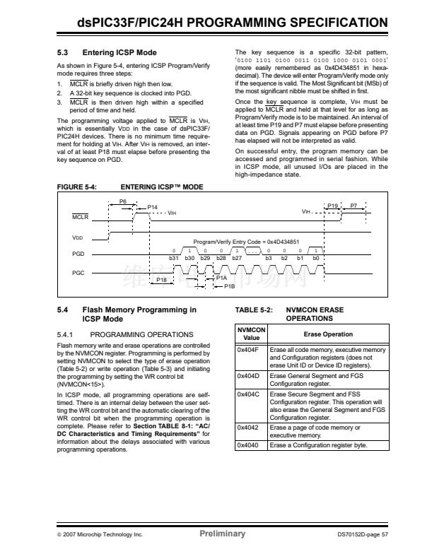
FIGURE 5-8:
VERIFY CODE
MEMORY FLOW
Start
5.12
Exiting ICSP Mode
Set TBLPTR = 0
Exiting Program/Verify mode is done by removing V
IH
from MCLR, as shown in Figure 5-9. The only require-
ment for exit is that an interval P16 should elapse
between the last clock and program signals on PGC
and PGD before removing V
IH
.
FIGURE 5-9:
EXITING ICSP鈩?MODE
P16
P17
V
IH
Read Low Byte
with Post-Increment
MCLR
V
DD
Read High Byte
with Post-Increment
PGD
PGC
V
IH
Does
Word = Expect
Data?
Yes
No
All
code memory
verified?
Yes
Done
No
Failure,
Report
Error
PGD = Input
DS70152D-page 66
Preliminary
漏
2007 Microchip Technology Inc.


 1
1
 2
2
 3
3
 4
4
 5
5
 6
6
 7
7
 8
8
 9
9
 10
10
 11
11
 12
12
 13
13
 14
14
 15
15
 16
16
 17
17
 18
18
 19
19
 20
20
 21
21
 22
22
 23
23
 24
24
 25
25
 26
26
 27
27
 28
28
 29
29
 30
30
 31
31
 32
32
 33
33
 34
34
 35
35
 36
36
 37
37
 38
38
 39
39
 40
40
 41
41
 42
42
 43
43
 44
44
 45
45
 46
46
 47
47
 48
48
 49
49
 50
50
 51
51
 52
52
 53
53
 54
54
 55
55
 56
56
 57
57
 58
58
 59
59
 60
60
 61
61
 62
62
 63
63
 64
64
 65
65
 66
66
 67
67
 68
68
 69
69
 70
70
 71
71
 72
72
 73
73
 74
74
 75
75
 76
76
 77
77
 78
78
 79
79
 80
80
