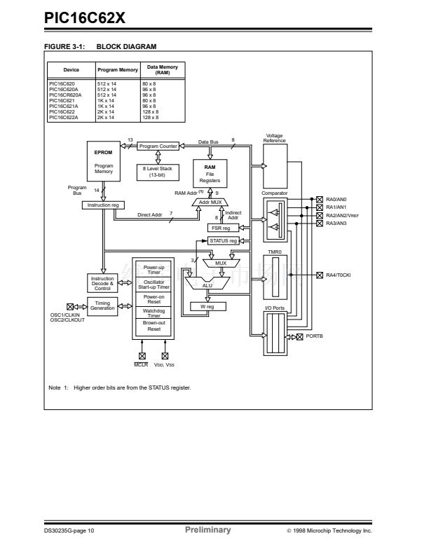
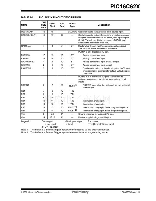
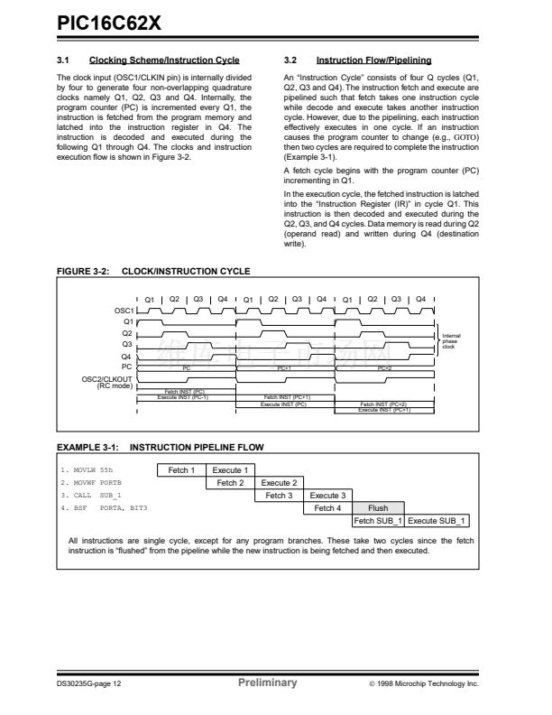
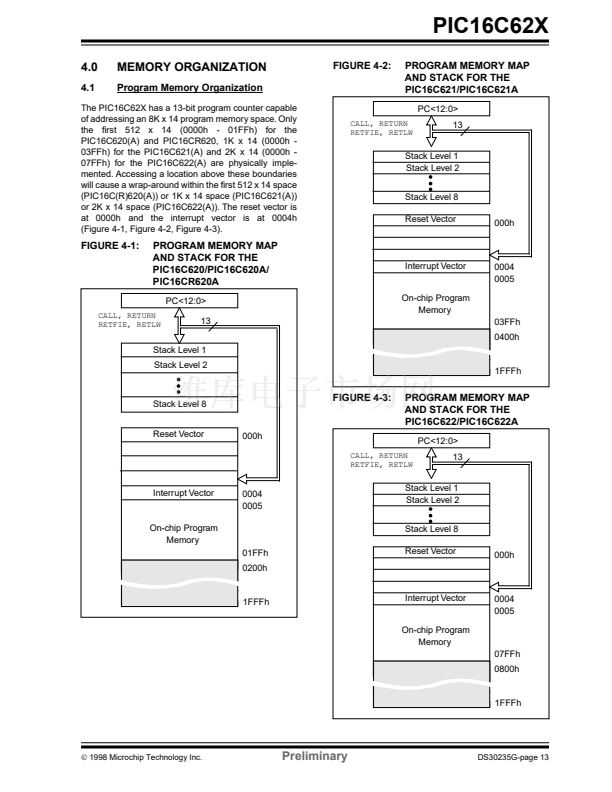
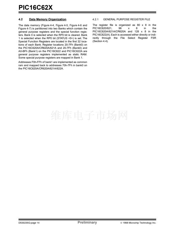
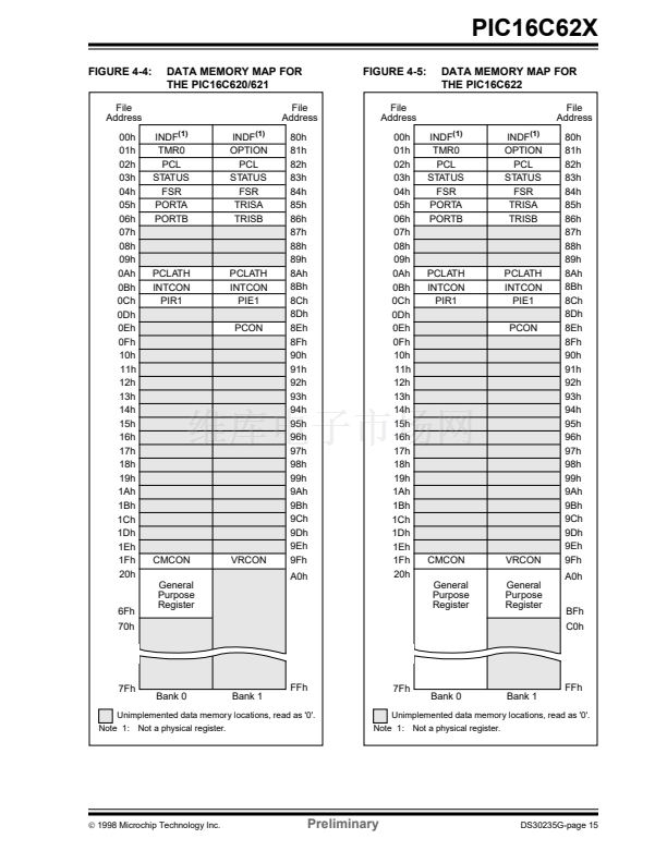
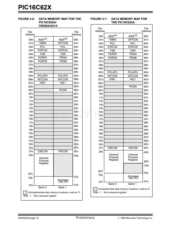
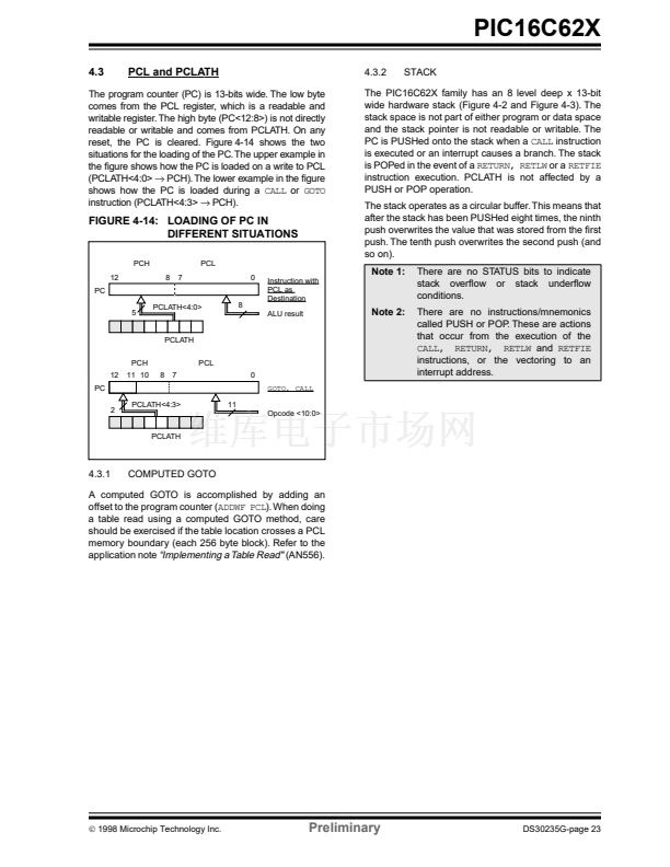
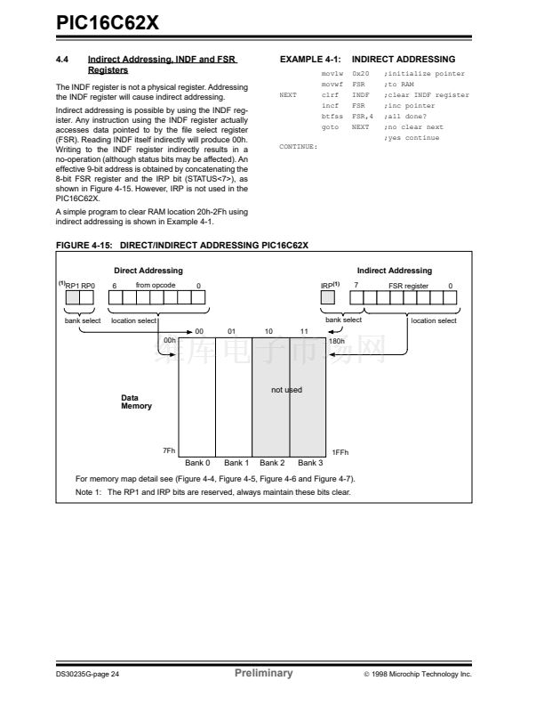
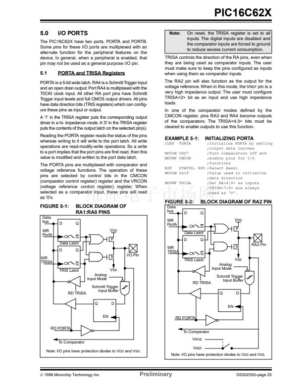
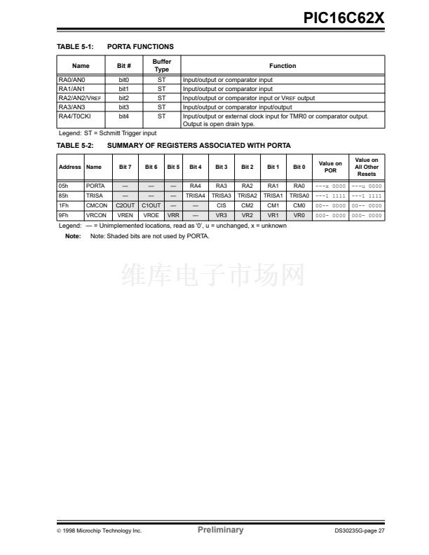
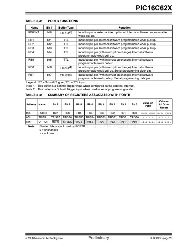
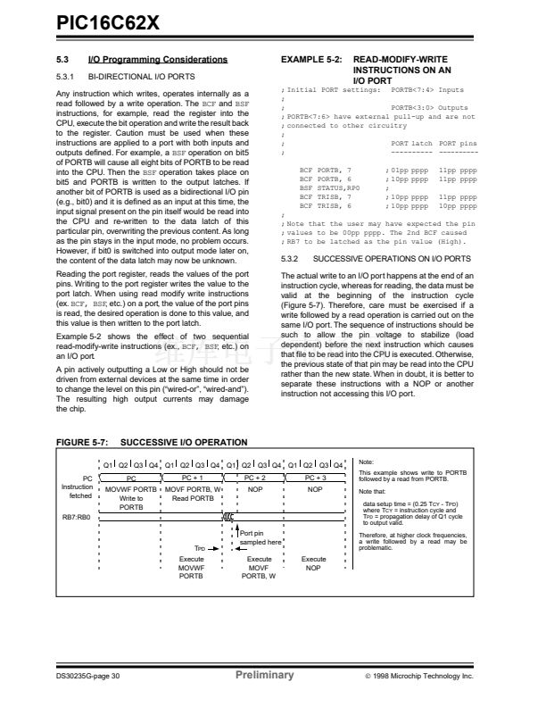
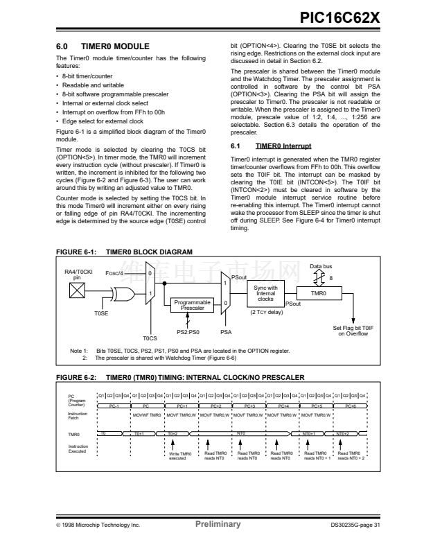
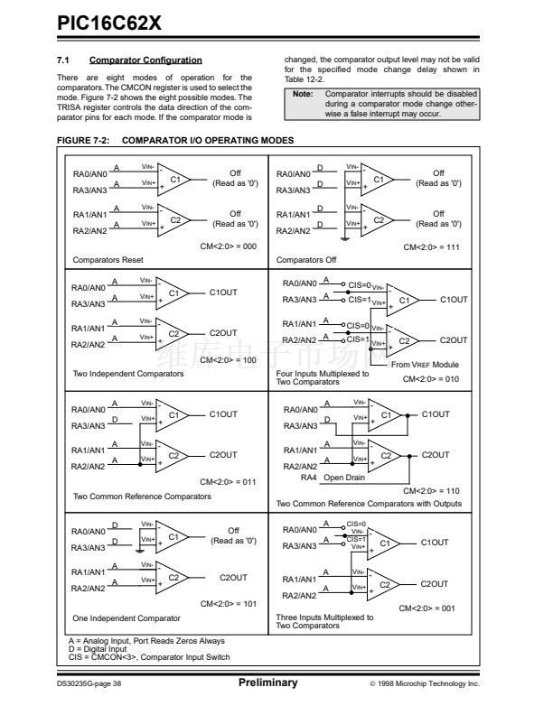
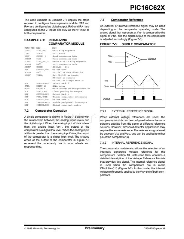
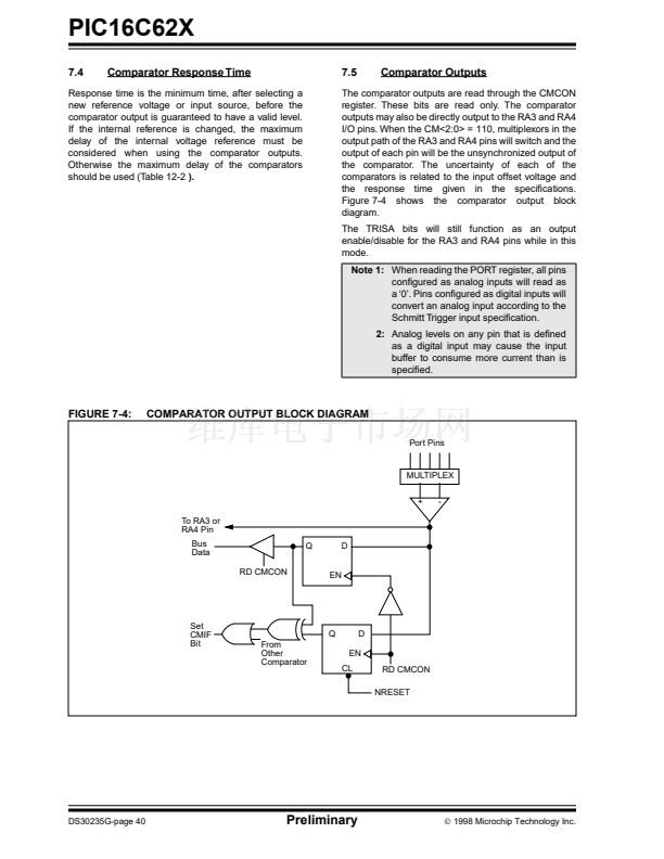
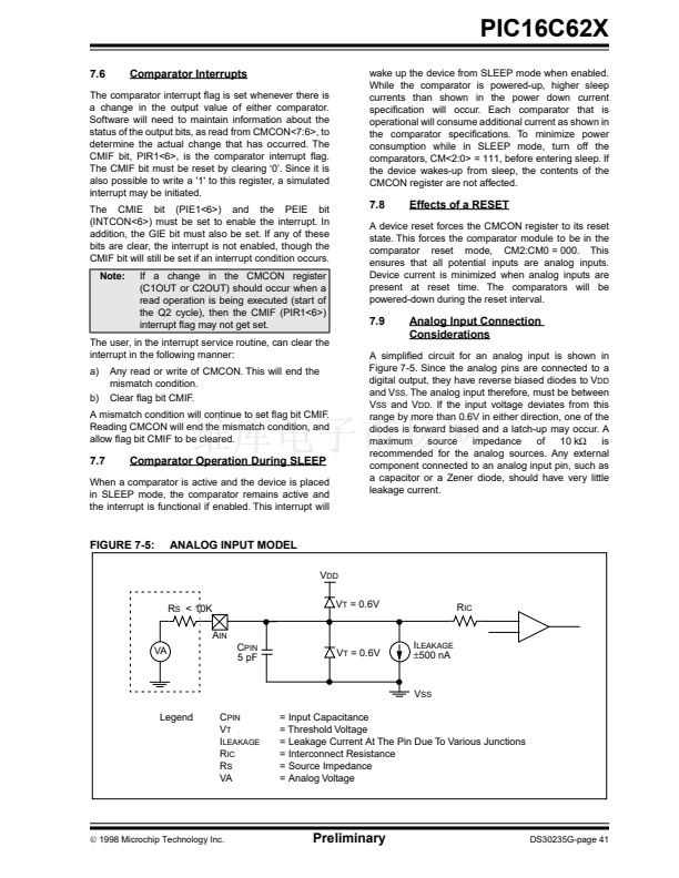
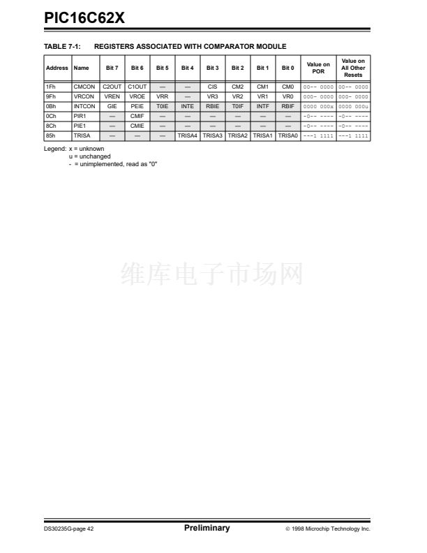
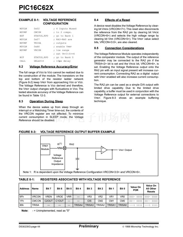
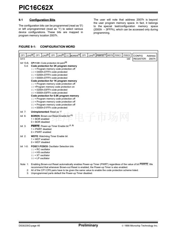
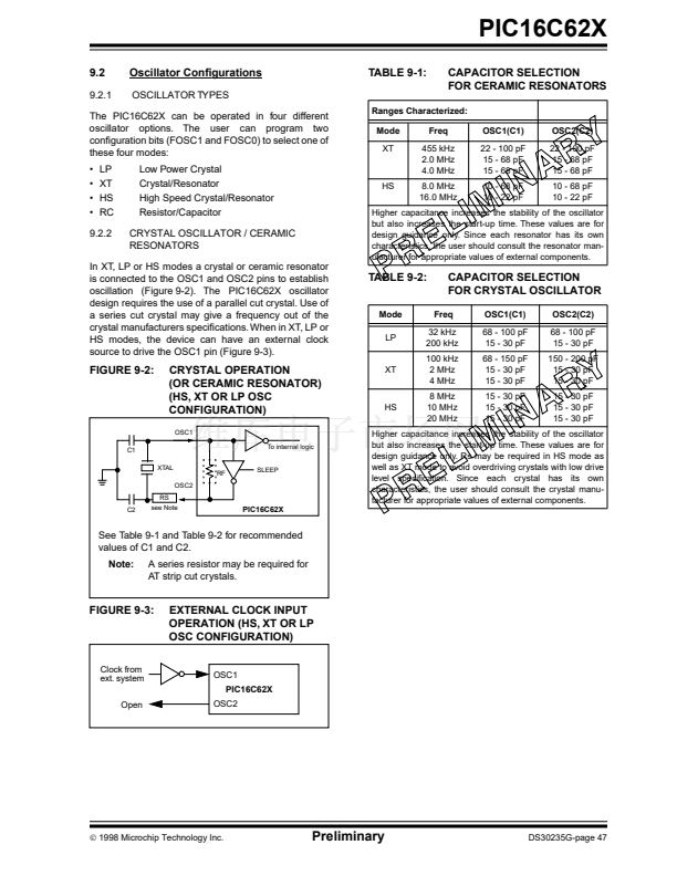
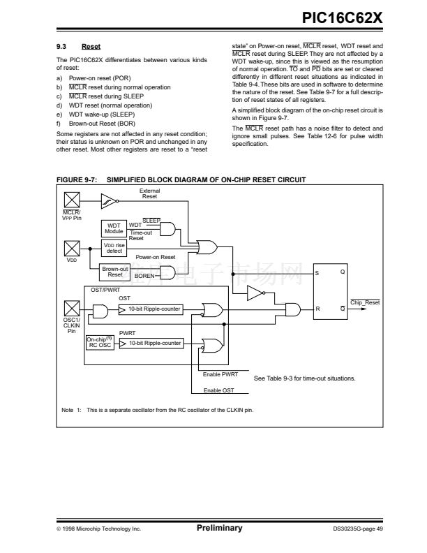
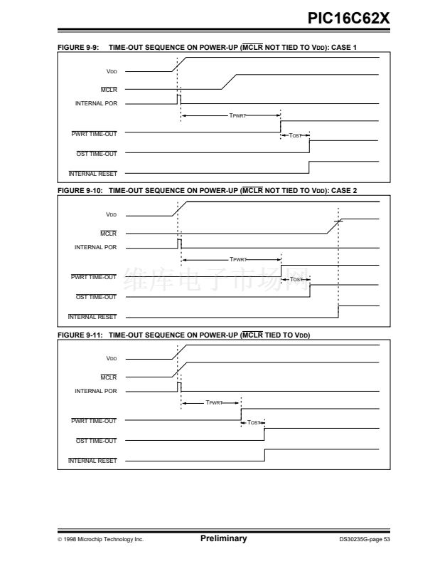
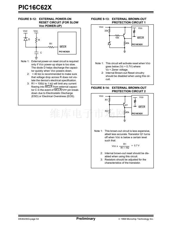
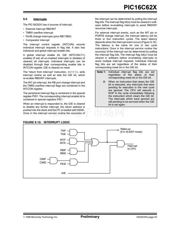
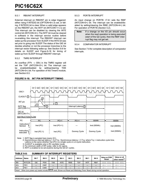
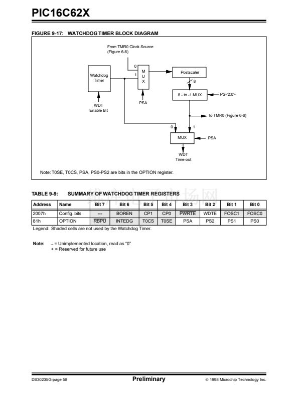
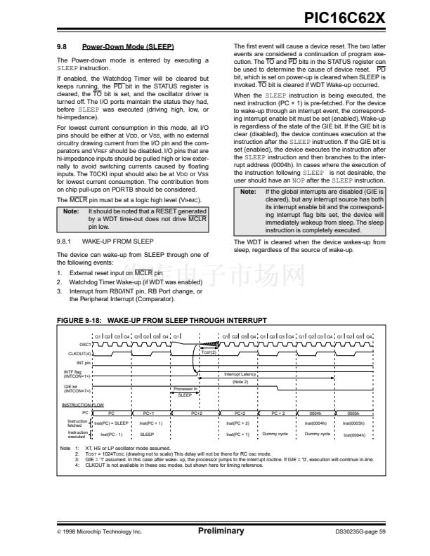
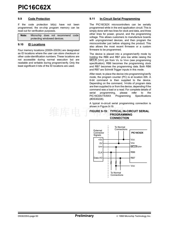
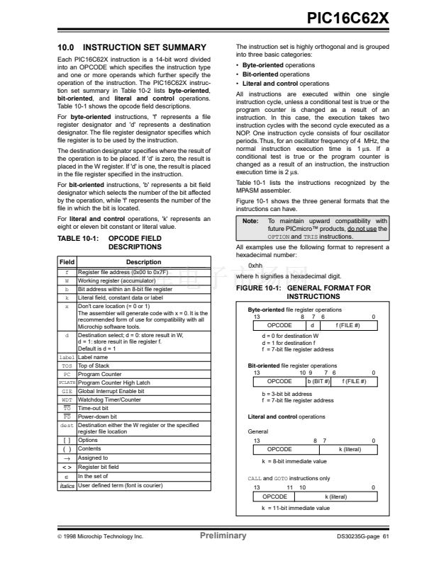
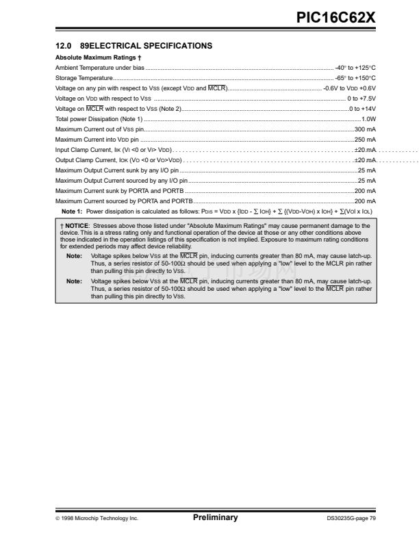
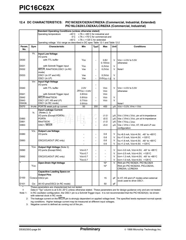
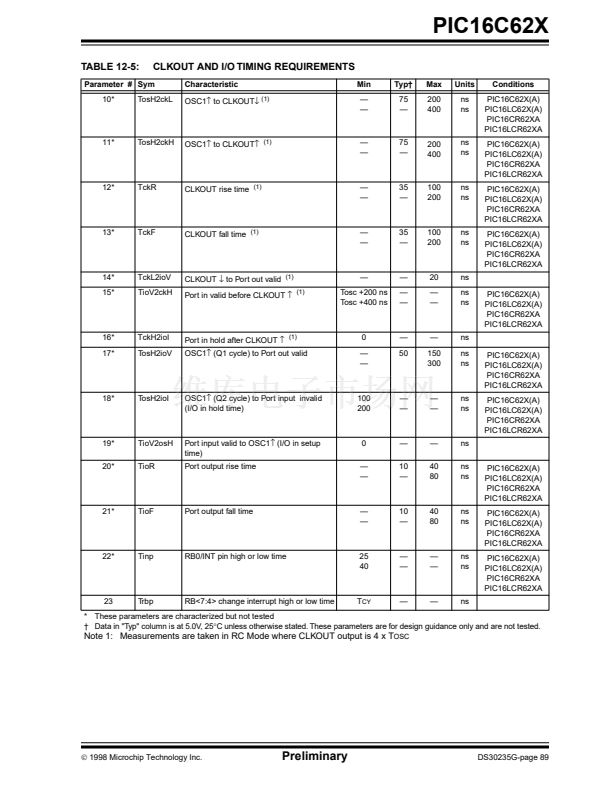
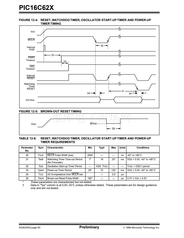
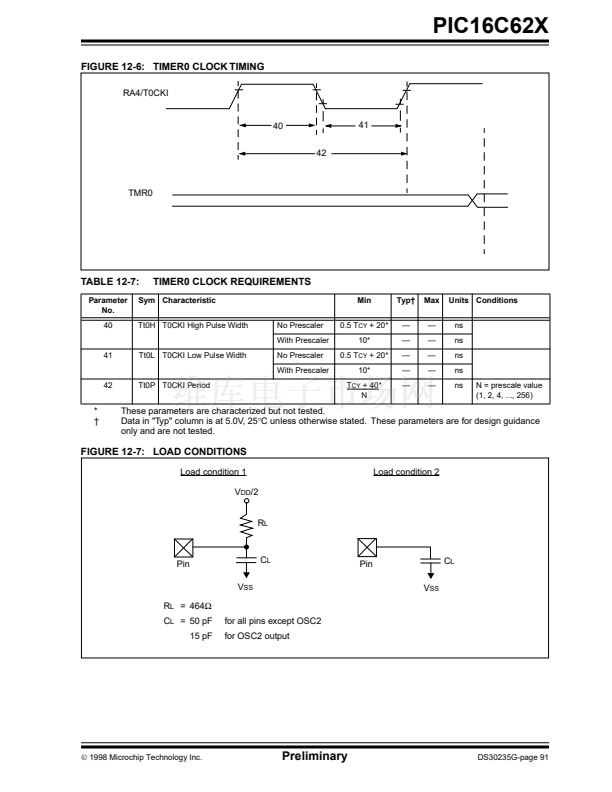
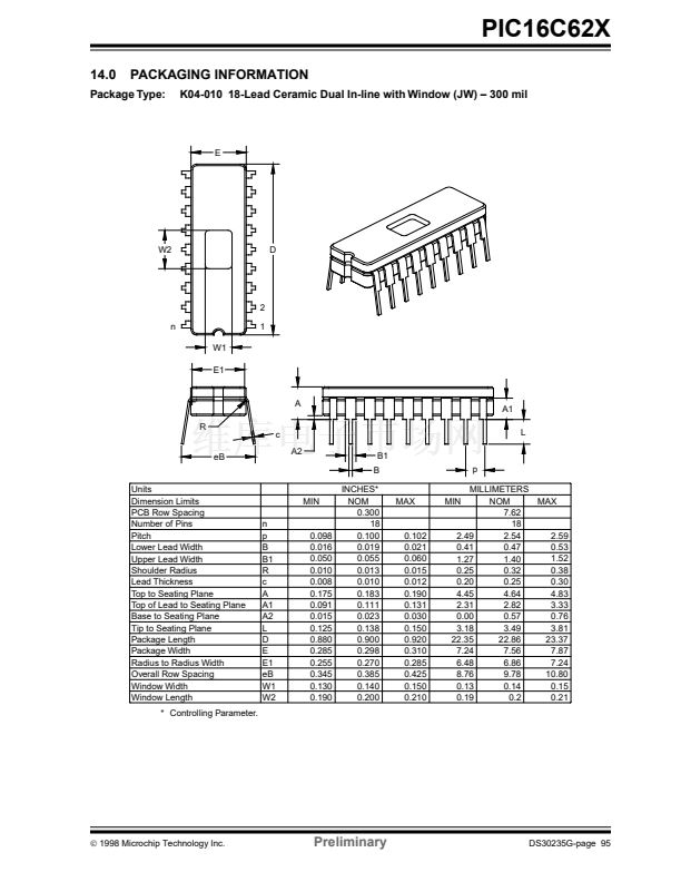
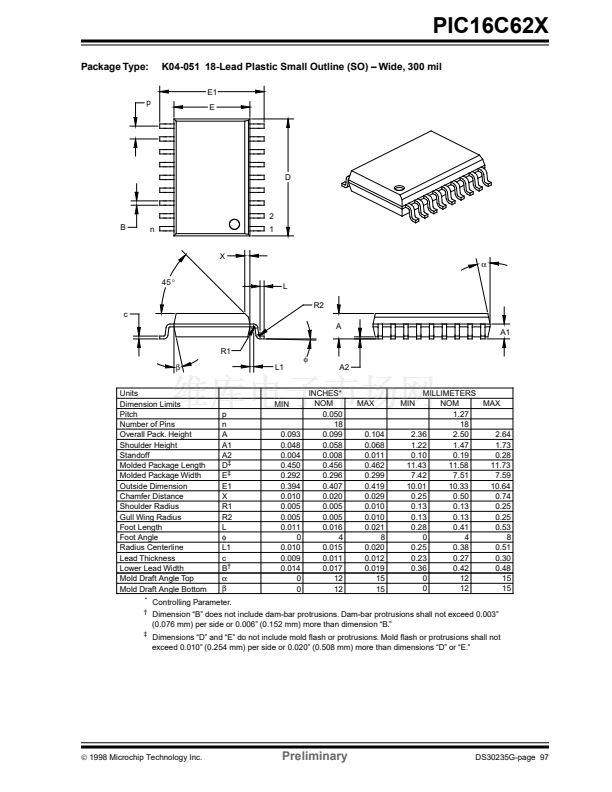
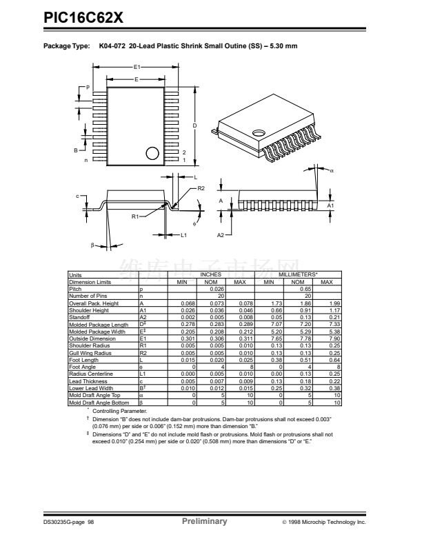
PIC16C62X
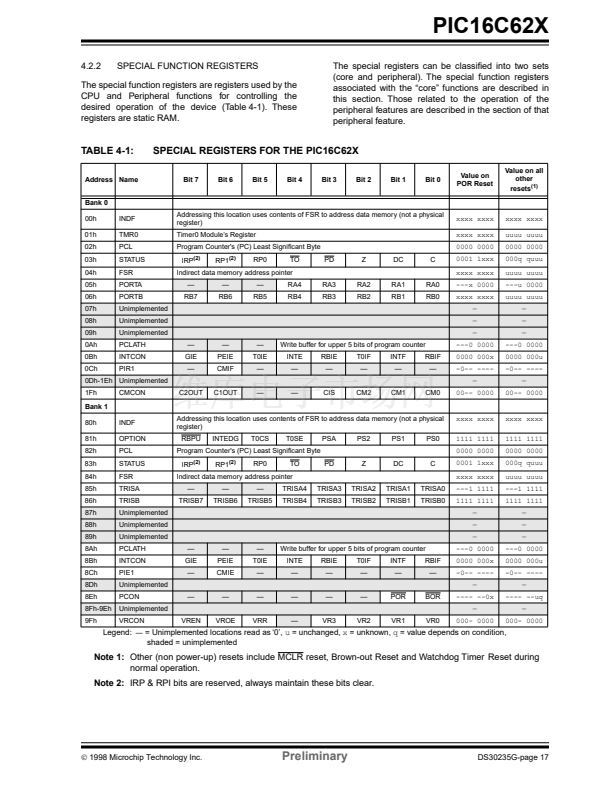
4.2.2.2
OPTION REGISTER
Note:
To achieve a 1:1 prescaler assignment for
TMR0, assign the prescaler to the WDT
(PSA = 1).
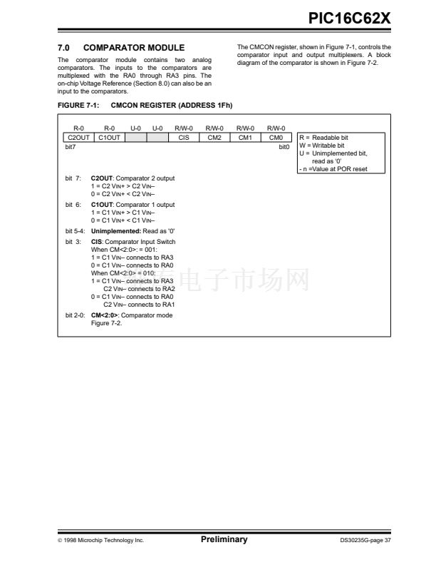
The OPTION register is a readable and writable
register which contains various control bits to con铿乬ure
the TMR0/WDT prescaler, the external RB0/INT
interrupt, TMR0, and the weak pull-ups on PORTB.
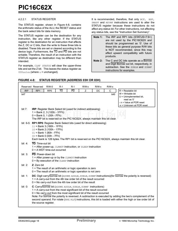
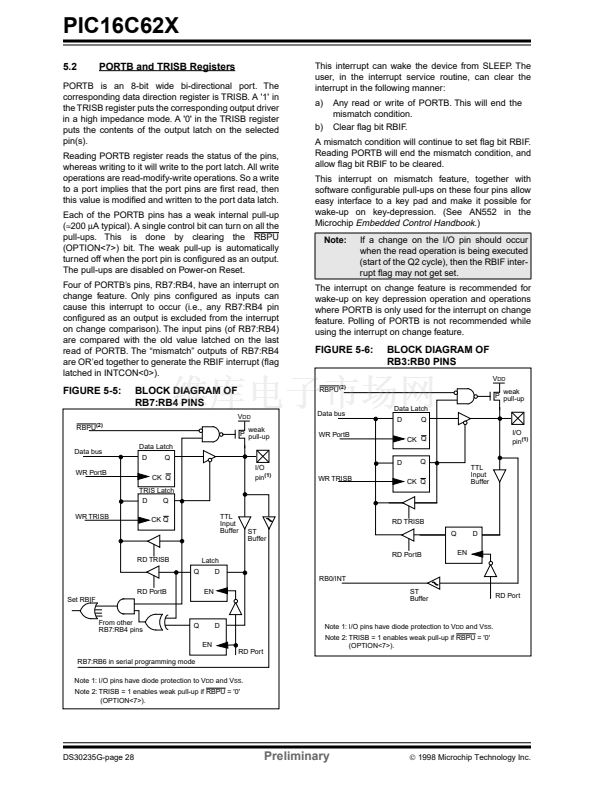
FIGURE 4-9:
R/W-1
RBPU
bit7
OPTION REGISTER (ADDRESS 81H)
R/W-1
T0CS
R/W-1
T0SE
R/W-1
PSA
R/W-1
PS2
R/W-1
PS1
R/W-1
PS0
bit0
R/W-1
INTEDG
R = Readable bit
W = Writable bit
- n = Value at POR reset
bit 7:
RBPU:
PORTB Pull-up Enable bit
1 = PORTB pull-ups are disabled
0 = PORTB pull-ups are enabled by individual port latch values
INTEDG:
Interrupt Edge Select bit
1 = Interrupt on rising edge of RB0/INT pin
0 = Interrupt on falling edge of RB0/INT pin
T0CS:
TMR0 Clock Source Select bit
1 = Transition on RA4/T0CKI pin
0 = Internal instruction cycle clock (CLKOUT)
T0SE:
TMR0 Source Edge Select bit
1 = Increment on high-to-low transition on RA4/T0CKI pin
0 = Increment on low-to-high transition on RA4/T0CKI pin
PSA:
Prescaler Assignment bit
1 = Prescaler is assigned to the WDT
0 = Prescaler is assigned to the Timer0 module
bit 6:
bit 5:
bit 4:
bit 3:
bit 2-0:
PS2:PS0:
Prescaler Rate Select bits
Bit Value
000
001
010
011
100
101
110
111
TMR0 Rate
1:2
1:4
1:8
1 : 16
1 : 32
1 : 64
1 : 128
1 : 256
WDT Rate
1:1
1:2
1:4
1:8
1 : 16
1 : 32
1 : 64
1 : 128
漏
1998 Microchip Technology Inc.
Preliminary
DS30235G-page 19


 1
1
 2
2
 3
3
 4
4
 5
5
 6
6
 7
7
 8
8
 9
9
 10
10
 11
11
 12
12
 13
13
 14
14
 15
15
 16
16
 17
17
 18
18
 19
19
 20
20
 21
21
 22
22
 23
23
 24
24
 25
25
 26
26
 27
27
 28
28
 29
29
 30
30
 31
31
 32
32
 33
33
 34
34
 35
35
 36
36
 37
37
 38
38
 39
39
 40
40
 41
41
 42
42
 43
43
 44
44
 45
45
 46
46
 47
47
 48
48
 49
49
 50
50
 51
51
 52
52
 53
53
 54
54
 55
55
 56
56
 57
57
 58
58
 59
59
 60
60
 61
61
 62
62
 63
63
 64
64
 65
65
 66
66
 67
67
 68
68
 69
69
 70
70
 71
71
 72
72
 73
73
 74
74
 75
75
 76
76
 77
77
 78
78
 79
79
 80
80
 81
81
 82
82
 83
83
 84
84
 85
85
 86
86
 87
87
 88
88
 89
89
 90
90
 91
91
 92
92
 93
93
 94
94
 95
95
 96
96
 97
97
 98
98
 99
99
 100
100
 101
101
 102
102
 103
103
 104
104
 105
105
 106
106
 107
107
 108
108
