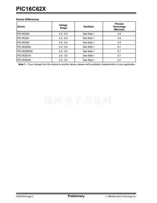
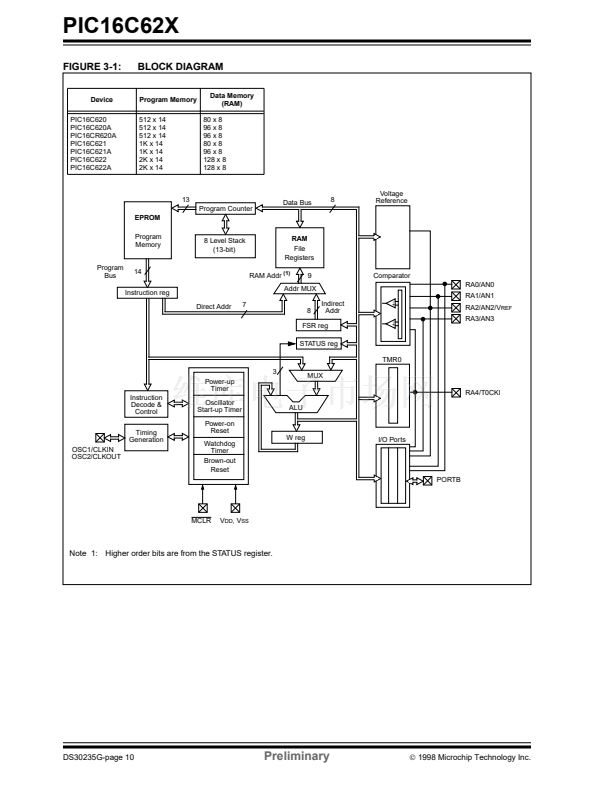
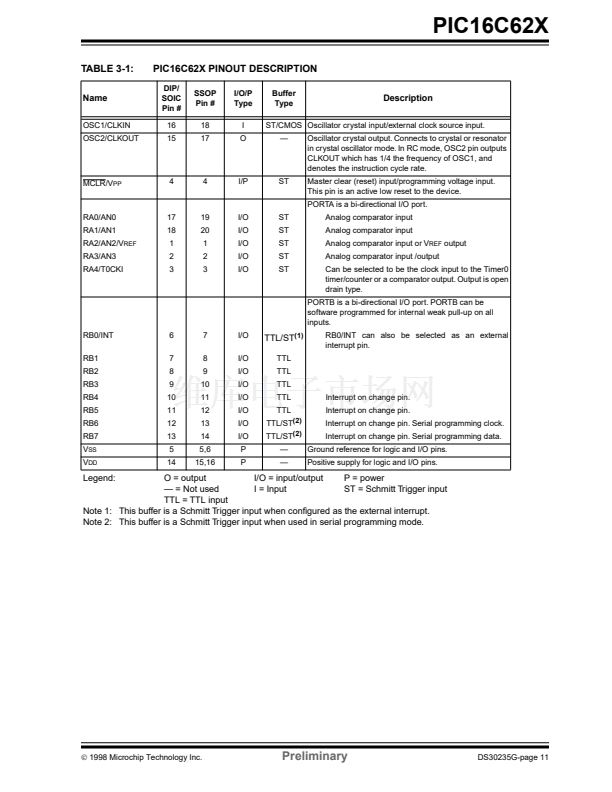
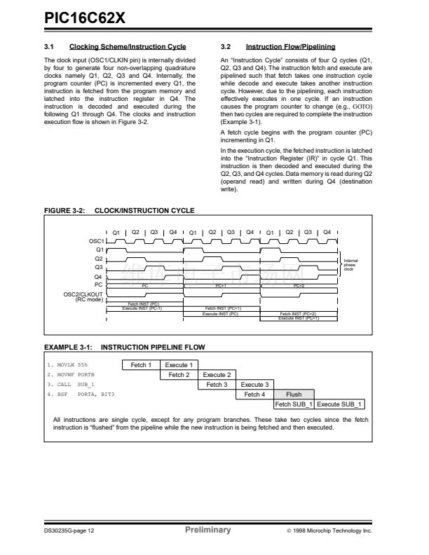
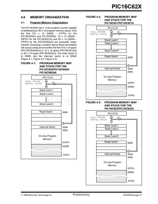
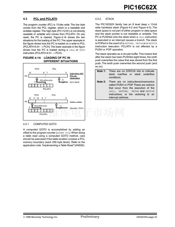
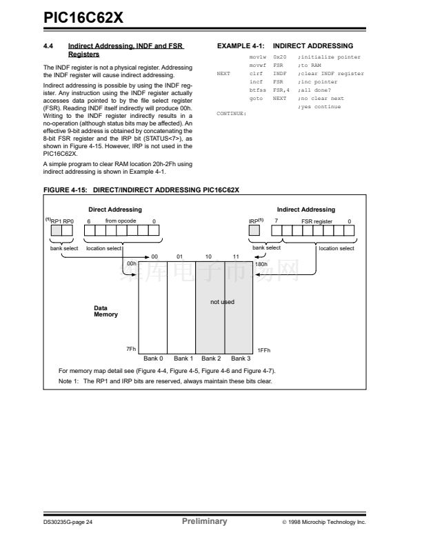
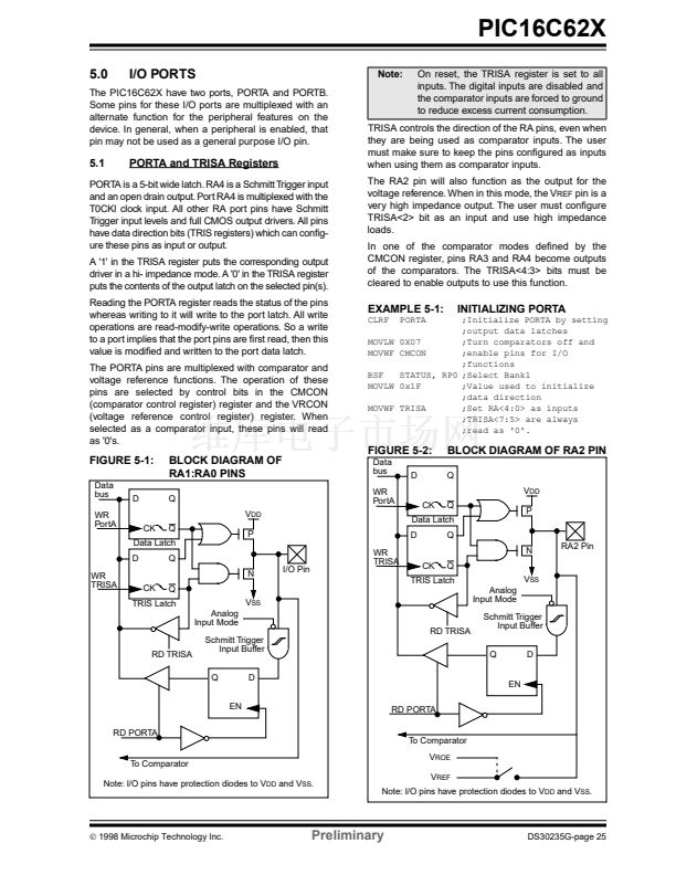
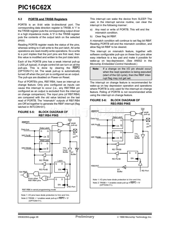
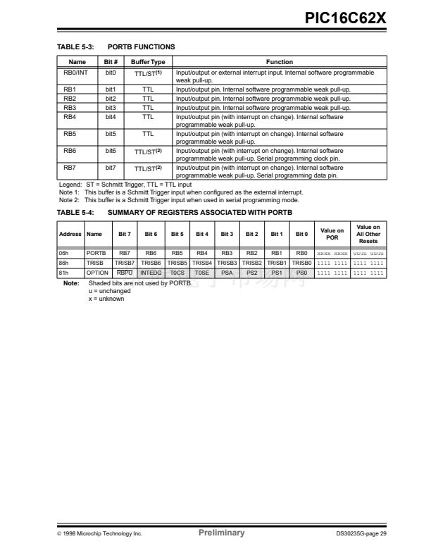
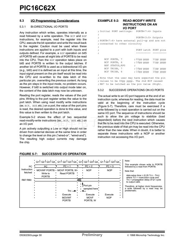
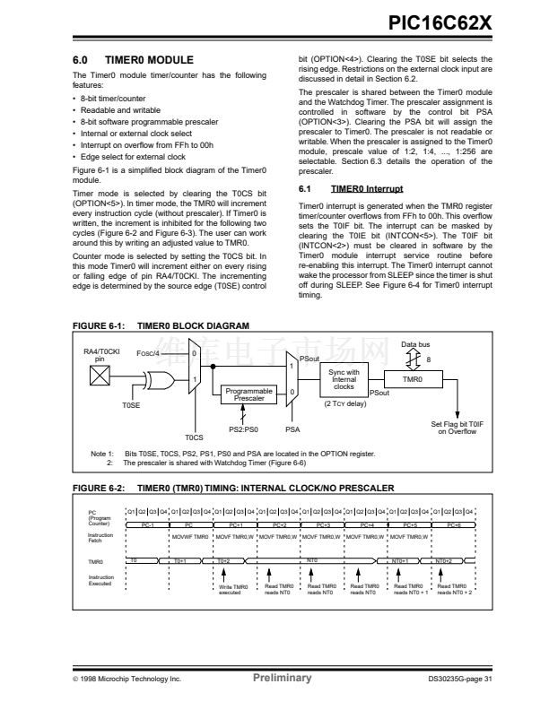
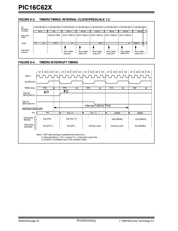
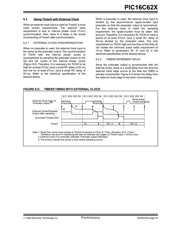
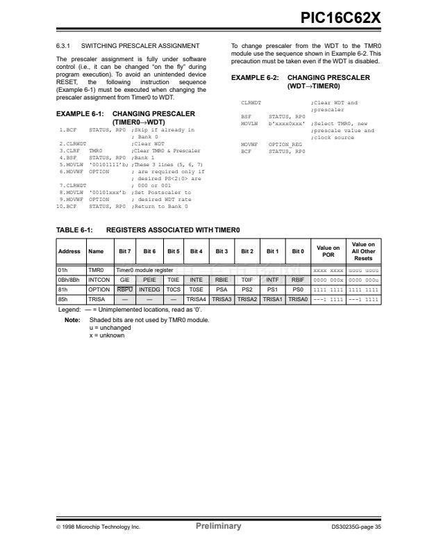
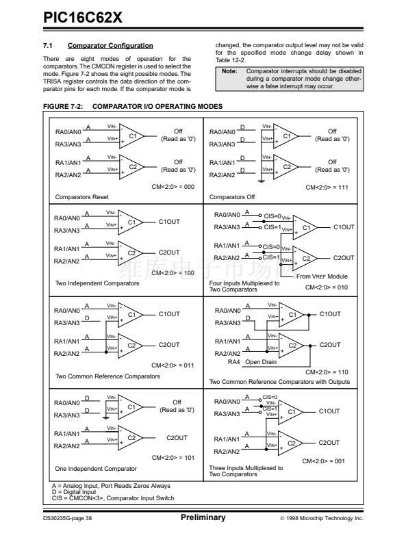
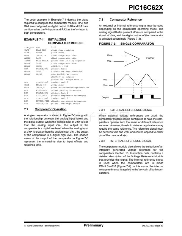
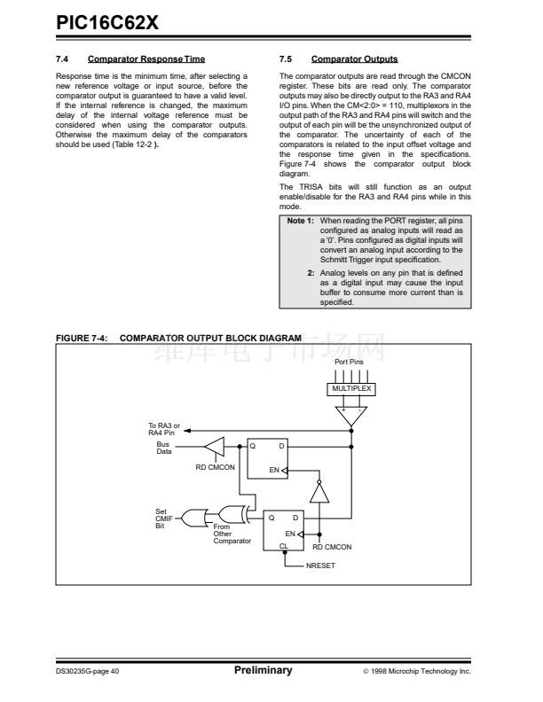
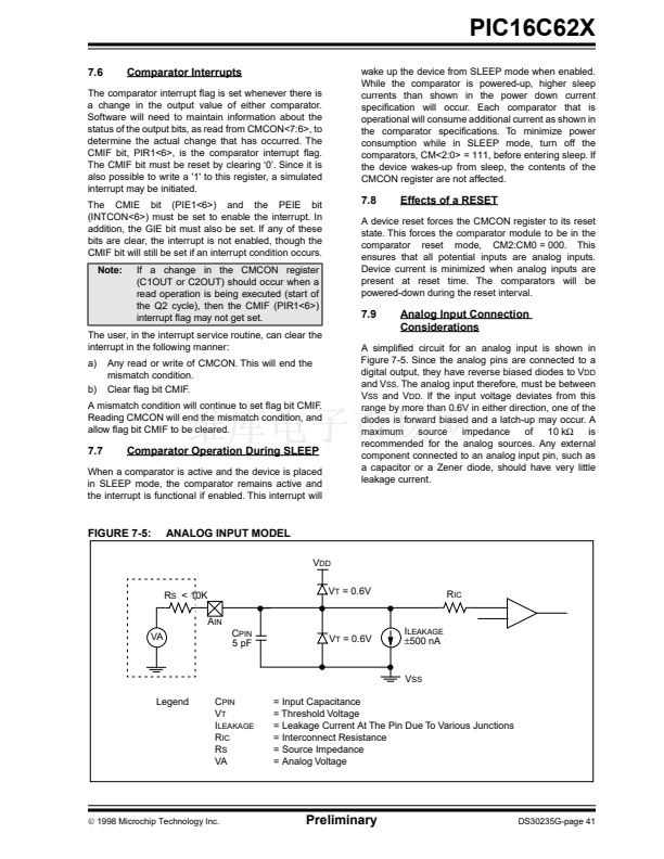
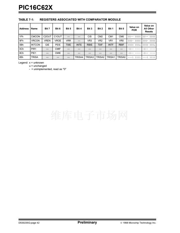
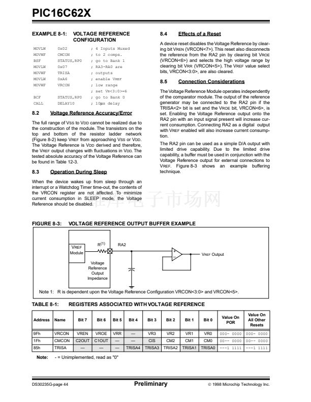
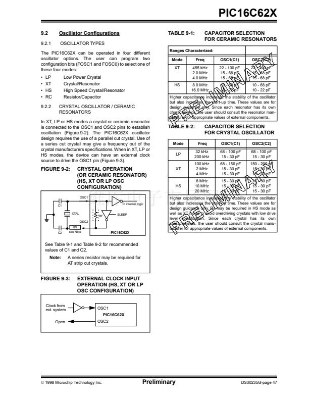
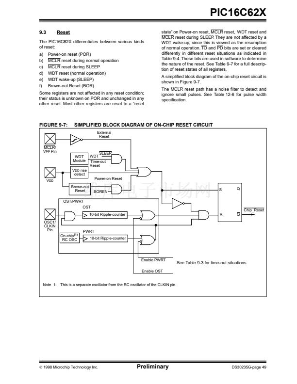
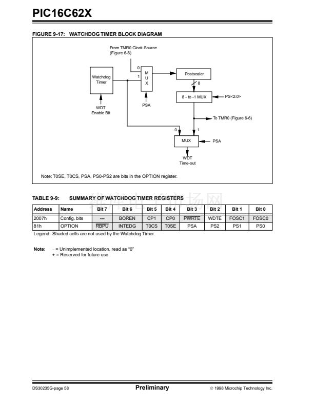
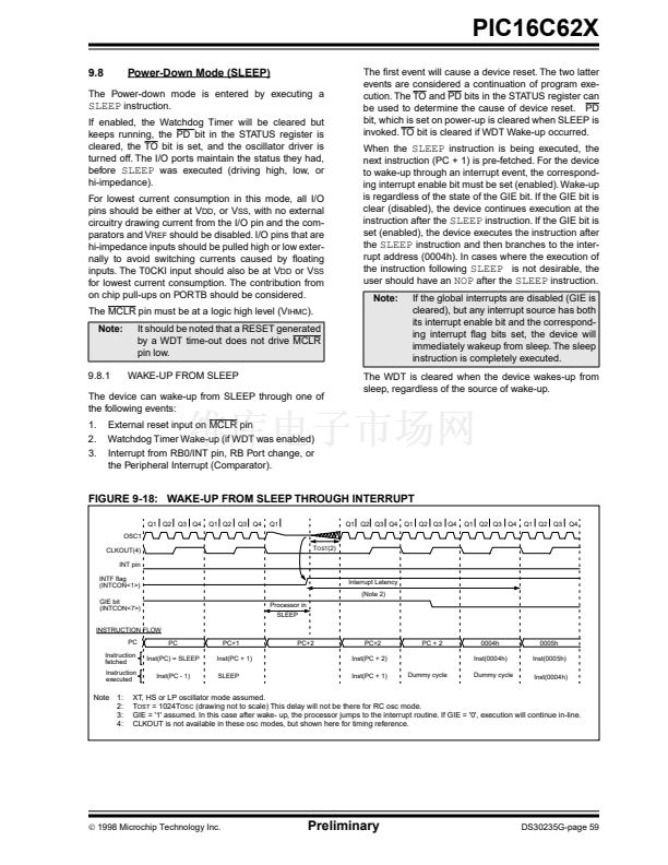
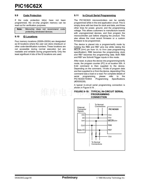
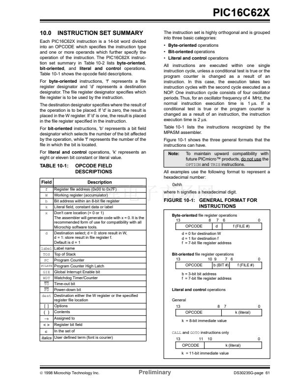
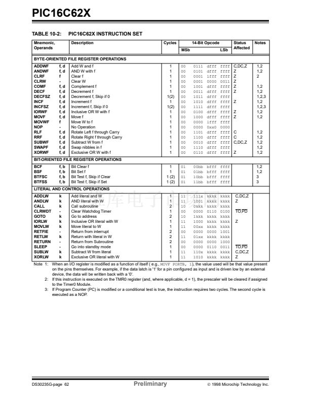
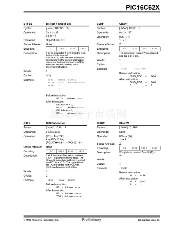
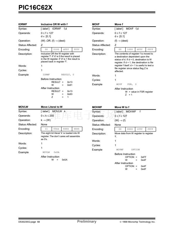
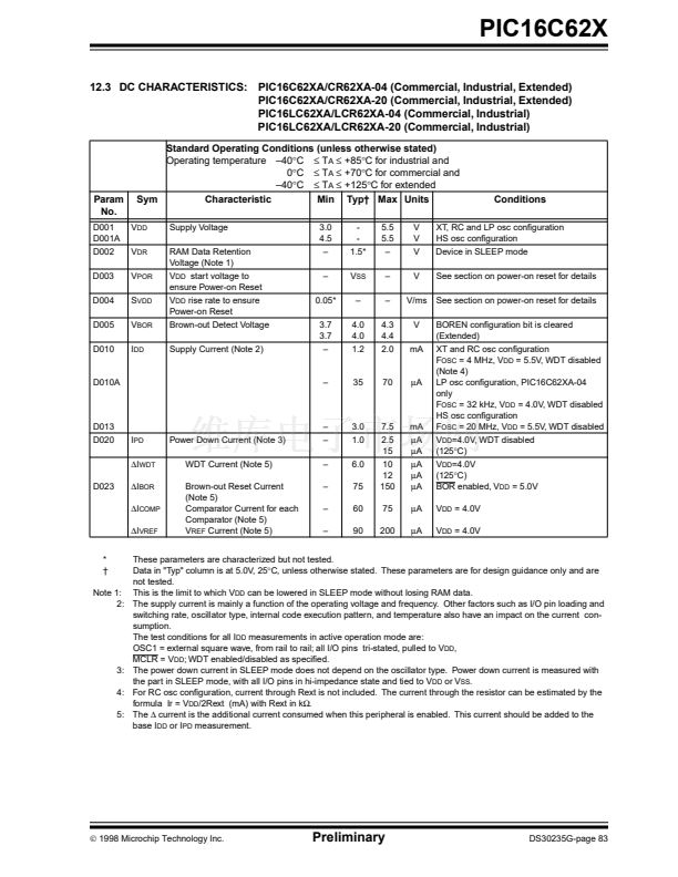
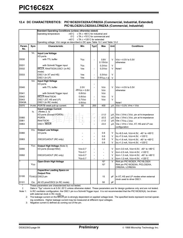
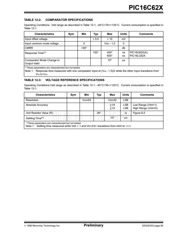
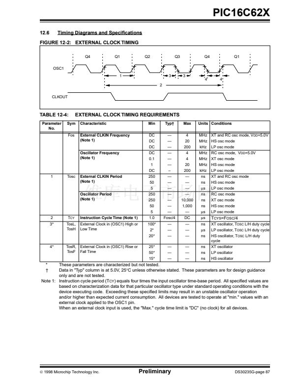
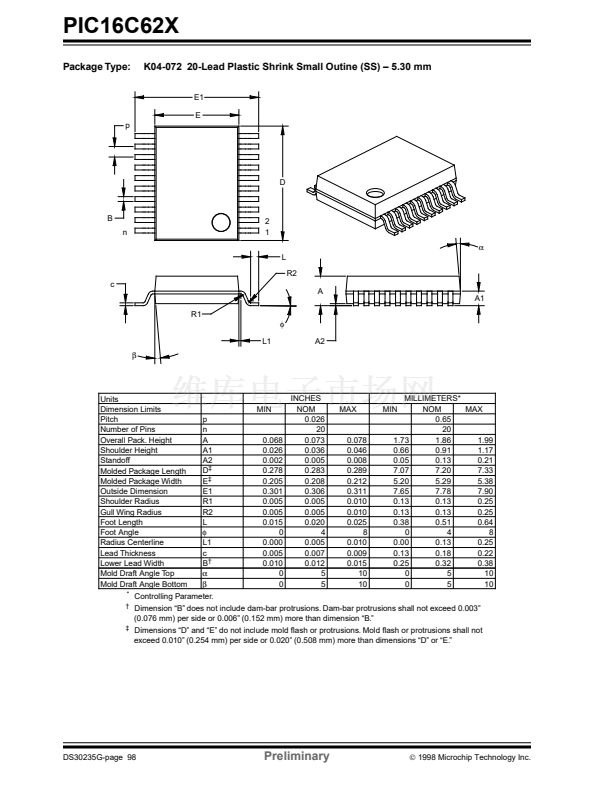
PIC16C62X
9.1
Con铿乬uration Bits
The con铿乬uration bits can be programmed (read as '0')
or left unprogrammed (read as '1') to select various
device con铿乬urations. These bits are mapped in
program memory location 2007h.
The user will note that address 2007h is beyond
the user program memory space. In fact, it belongs
to the special test/con铿乬uration memory space
(2000h 鈥?3FFFh), which can be accessed only during
programming.
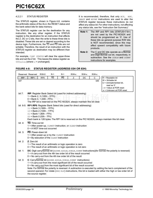
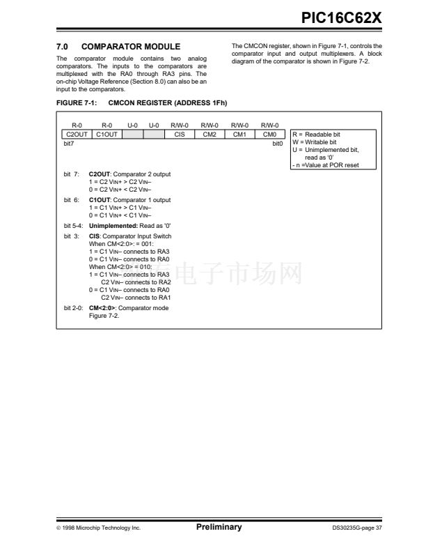
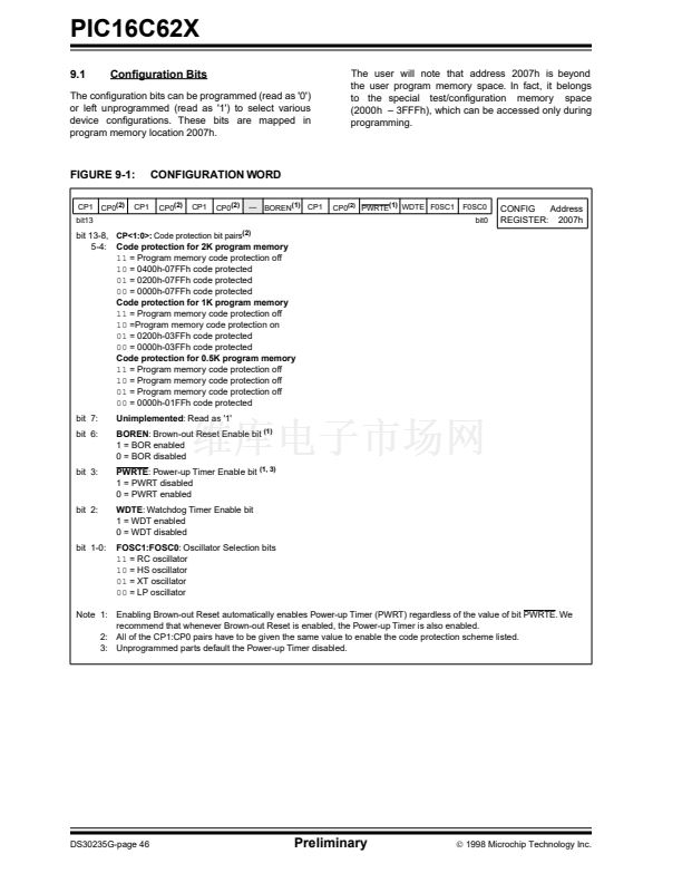
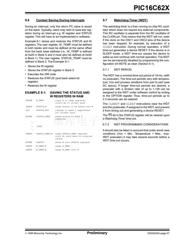
FIGURE 9-1:
CP1
CP0
(2)
CP1
CONFIGURATION WORD
CP0
(2)
CP1
CP0
(2)
鈥?BOREN
(1)
CP1
CP0
(2)
PWRTE
(1)
WDTE F0SC1
F0SC0
bit13
bit0
CONFIG
Address
REGISTER: 2007h
bit 13-8,
CP<1:0>:
Code protection bit pairs
(2)
5-4:
Code protection for 2K program memory
11
= Program memory code protection off
10
= 0400h-07FFh code protected
01
= 0200h-07FFh code protected
00
= 0000h-07FFh code protected
Code protection for 1K program memory
11
= Program memory code protection off
10
=Program memory code protection on
01
= 0200h-03FFh code protected
00
= 0000h-03FFh code protected
Code protection for 0.5K program memory
11
= Program memory code protection off
10
= Program memory code protection off
01
= Program memory code protection off
00
= 0000h-01FFh code protected
bit 7:
bit 6:
Unimplemented:
Read as '1'
BOREN:
Brown-out Reset Enable bit
(1)
1 = BOR enabled
0 = BOR disabled
PWRTE:
Power-up Timer Enable bit
(1, 3)
1 = PWRT disabled
0 = PWRT enabled
WDTE:
Watchdog Timer Enable bit
1 = WDT enabled
0 = WDT disabled
FOSC1:FOSC0:
Oscillator Selection bits
11
= RC oscillator
10
= HS oscillator
01
= XT oscillator
00
= LP oscillator
bit 3:
bit 2:
bit 1-0:
Note 1: Enabling Brown-out Reset automatically enables Power-up Timer (PWRT) regardless of the value of bit PWRTE. We
recommend that whenever Brown-out Reset is enabled, the Power-up Timer is also enabled.
2: All of the CP1:CP0 pairs have to be given the same value to enable the code protection scheme listed.
3: Unprogrammed parts default the Power-up Timer disabled.
DS30235G-page 46
Preliminary
漏
1998 Microchip Technology Inc.


 1
1
 2
2
 3
3
 4
4
 5
5
 6
6
 7
7
 8
8
 9
9
 10
10
 11
11
 12
12
 13
13
 14
14
 15
15
 16
16
 17
17
 18
18
 19
19
 20
20
 21
21
 22
22
 23
23
 24
24
 25
25
 26
26
 27
27
 28
28
 29
29
 30
30
 31
31
 32
32
 33
33
 34
34
 35
35
 36
36
 37
37
 38
38
 39
39
 40
40
 41
41
 42
42
 43
43
 44
44
 45
45
 46
46
 47
47
 48
48
 49
49
 50
50
 51
51
 52
52
 53
53
 54
54
 55
55
 56
56
 57
57
 58
58
 59
59
 60
60
 61
61
 62
62
 63
63
 64
64
 65
65
 66
66
 67
67
 68
68
 69
69
 70
70
 71
71
 72
72
 73
73
 74
74
 75
75
 76
76
 77
77
 78
78
 79
79
 80
80
 81
81
 82
82
 83
83
 84
84
 85
85
 86
86
 87
87
 88
88
 89
89
 90
90
 91
91
 92
92
 93
93
 94
94
 95
95
 96
96
 97
97
 98
98
 99
99
 100
100
 101
101
 102
102
 103
103
 104
104
 105
105
 106
106
 107
107
 108
108
