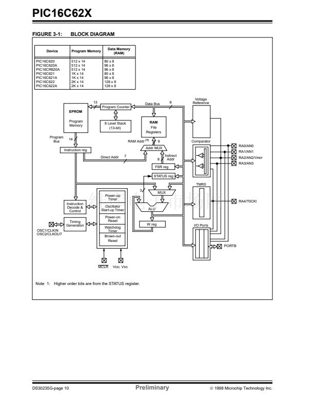
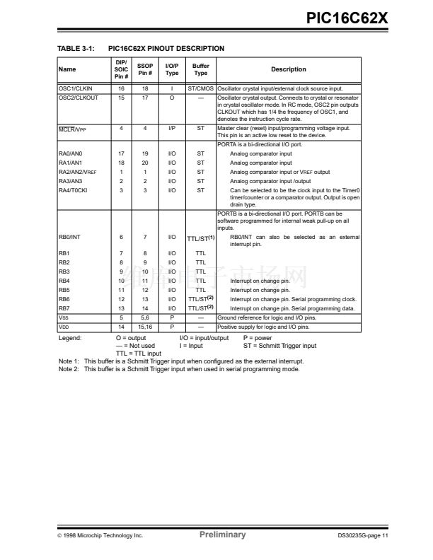
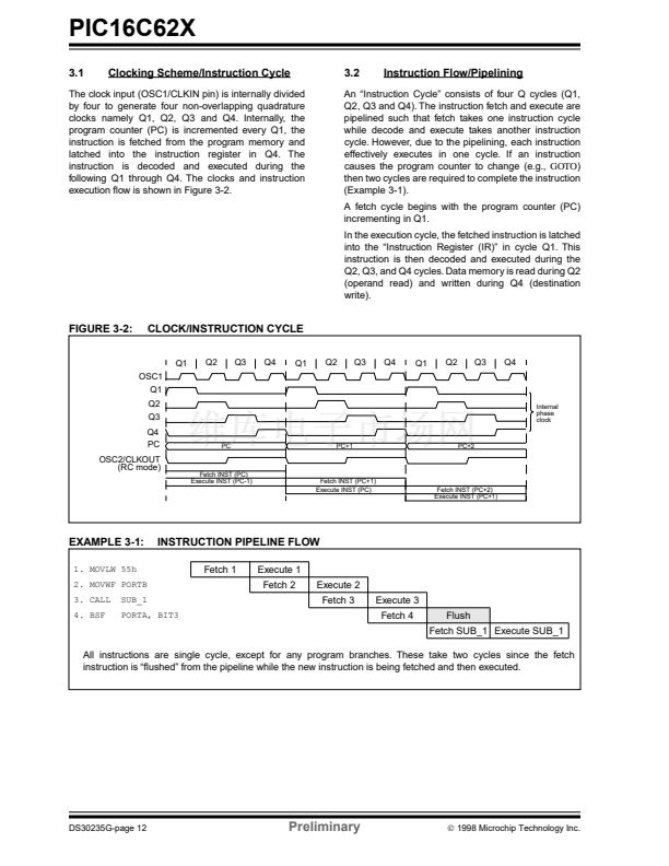
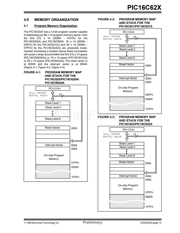
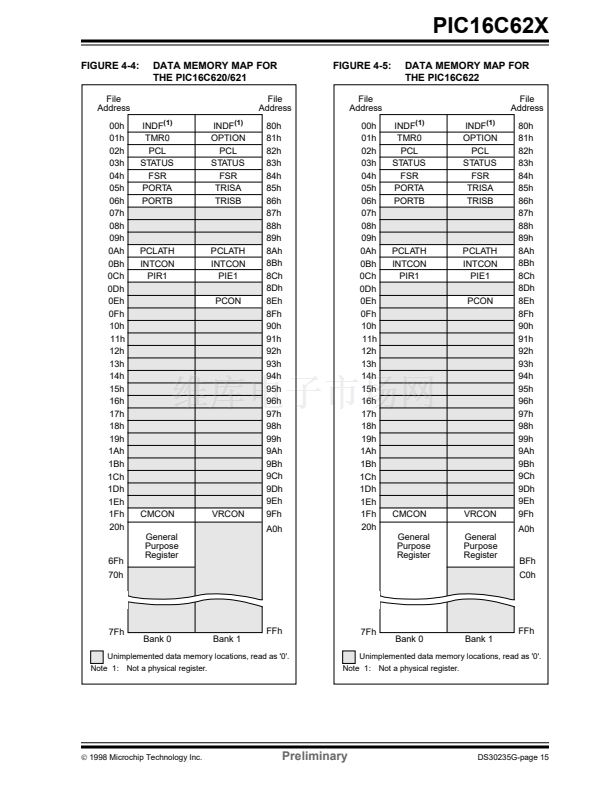
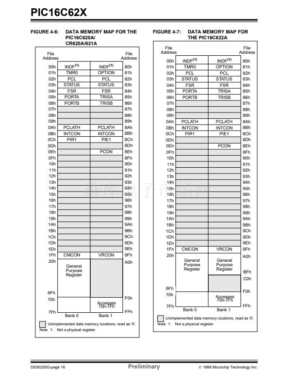
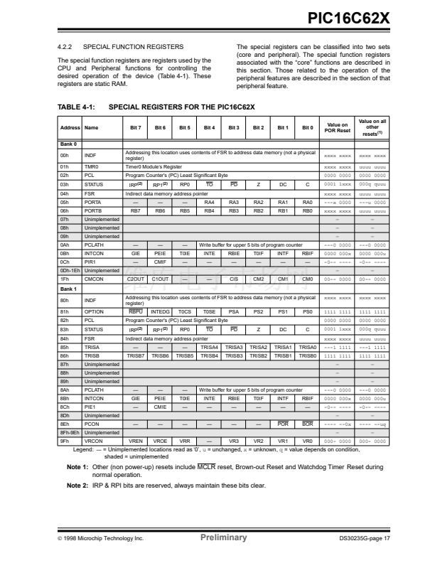
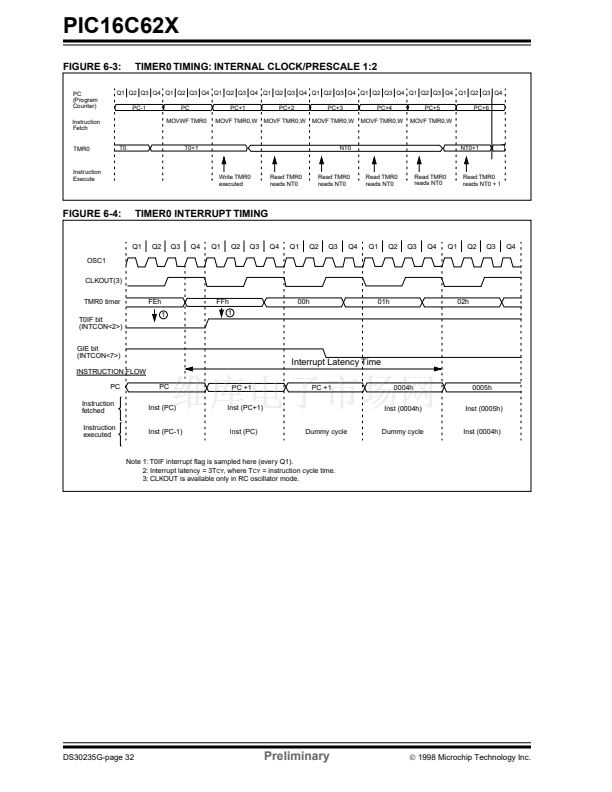
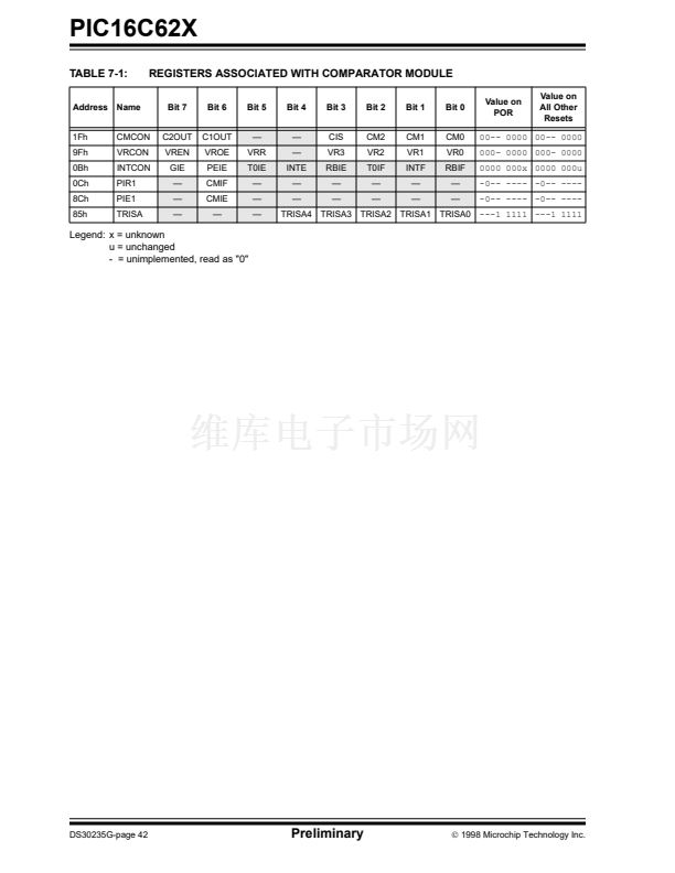
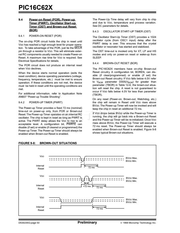
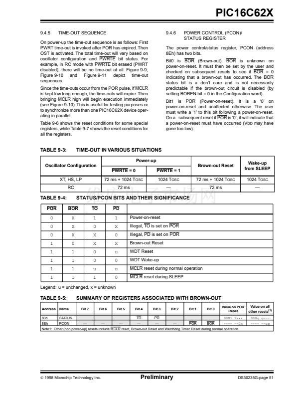
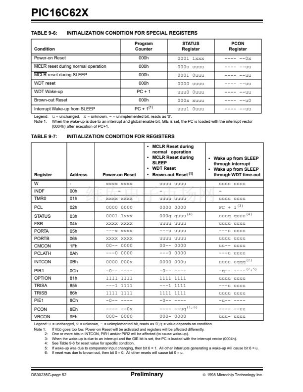
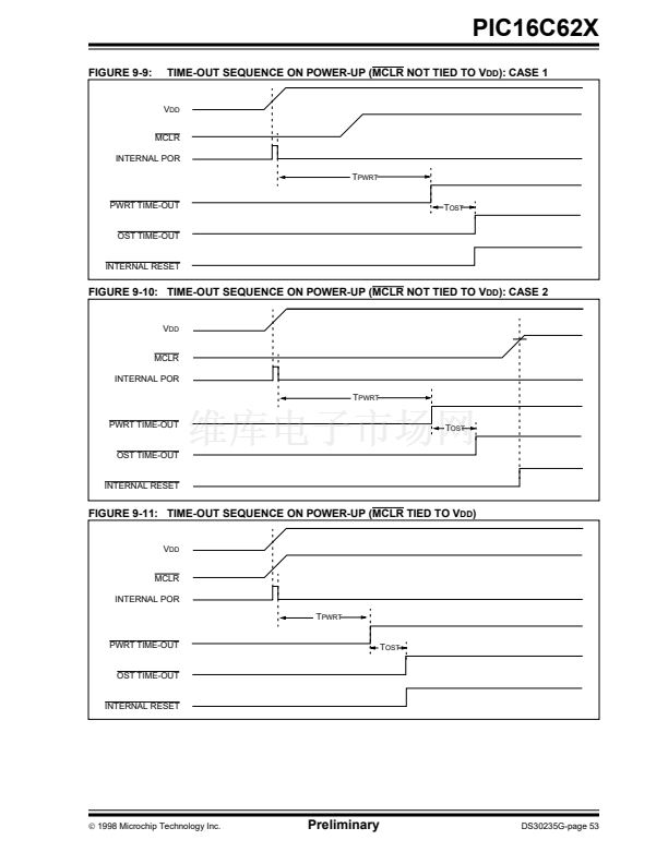
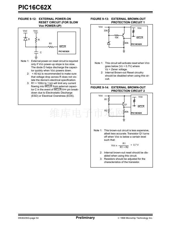
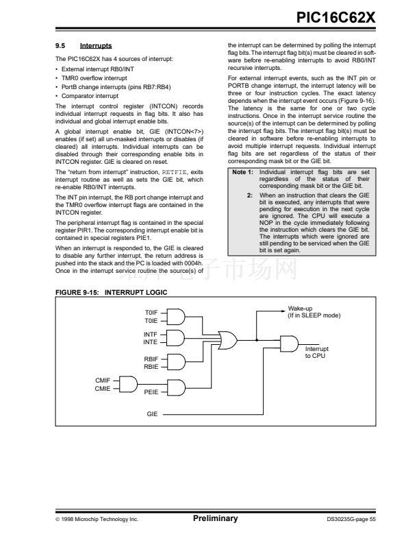
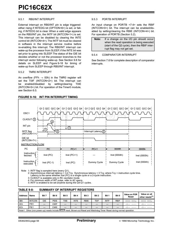
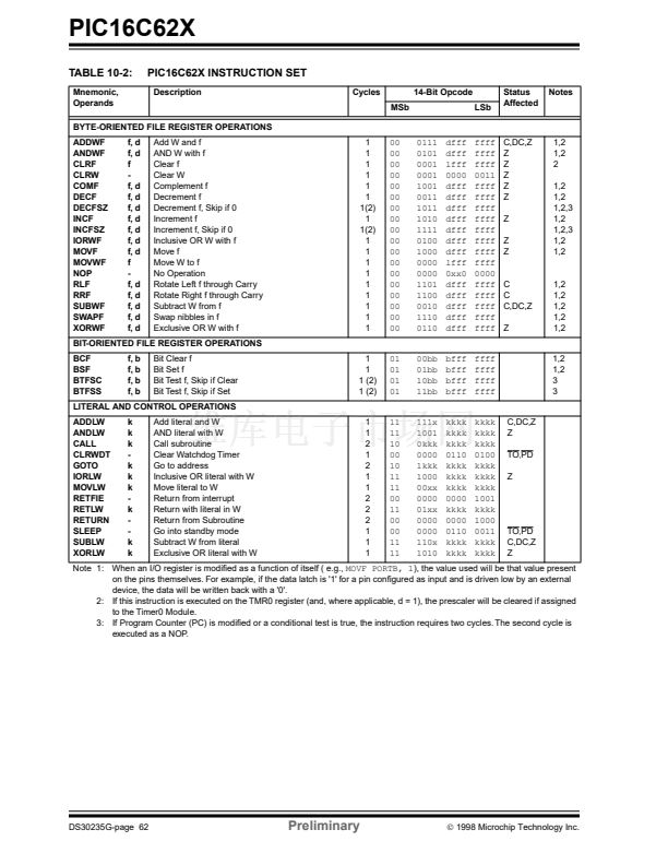
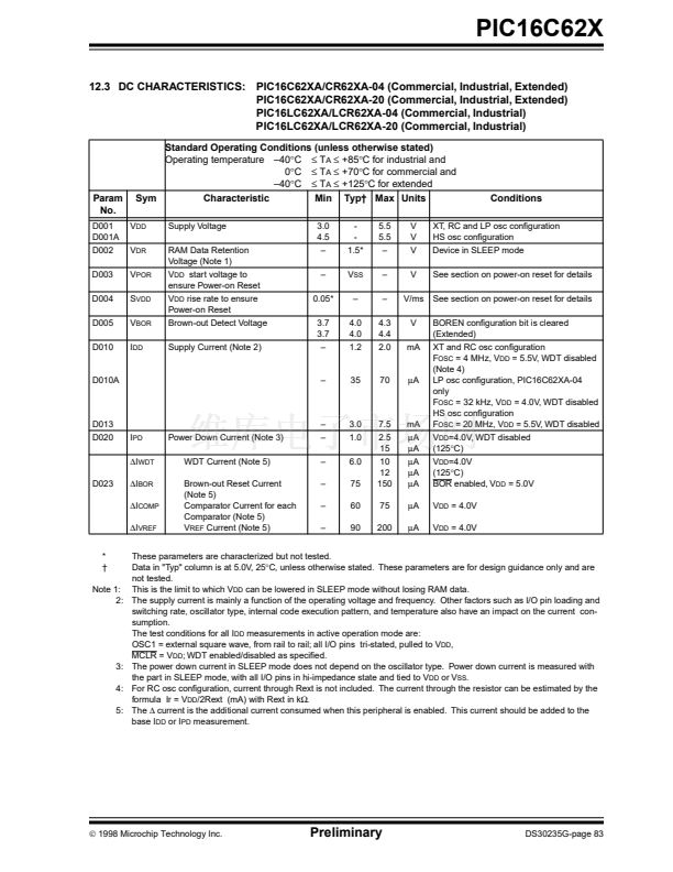
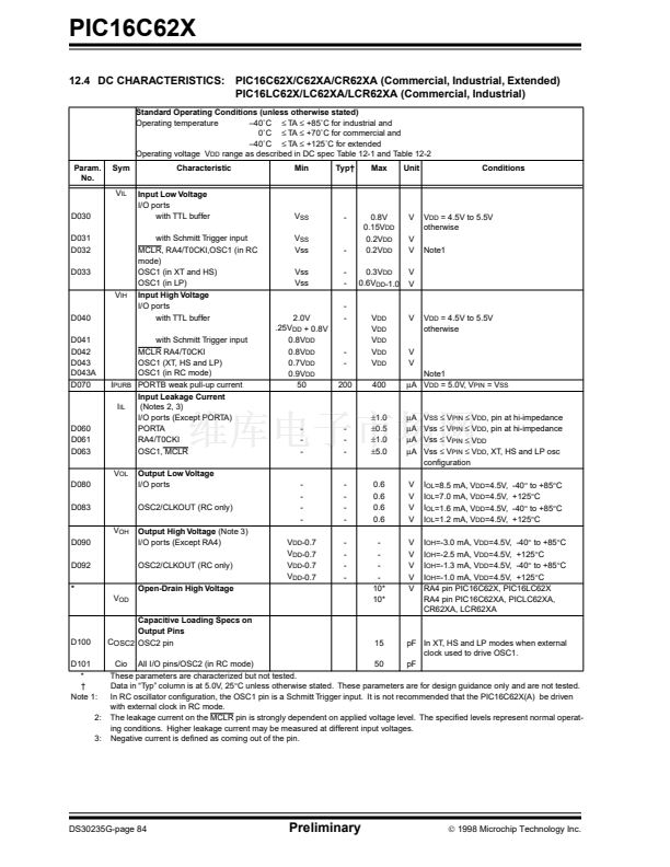
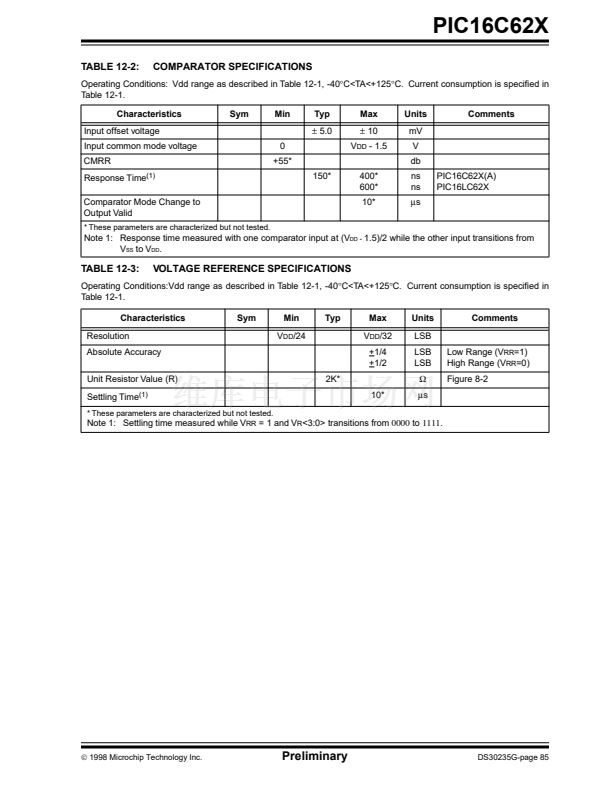
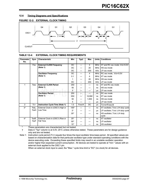
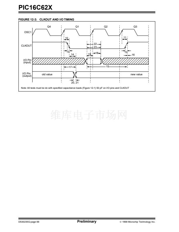
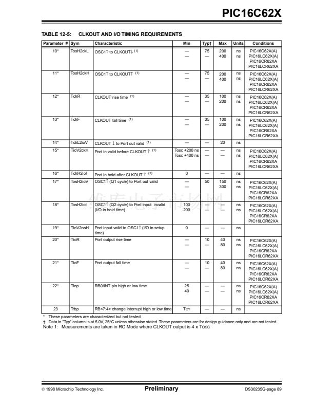
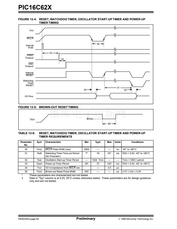
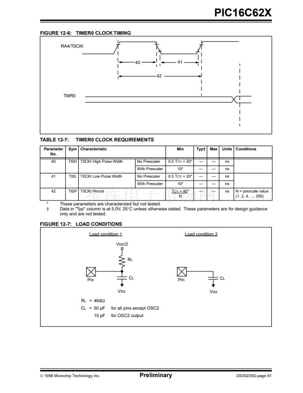
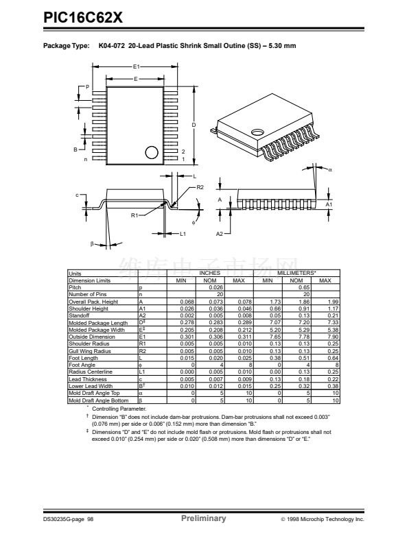
PIC16C62X
8.0
VOLTAGE REFERENCE
MODULE
8.1
Con铿乬uring the Voltage Reference
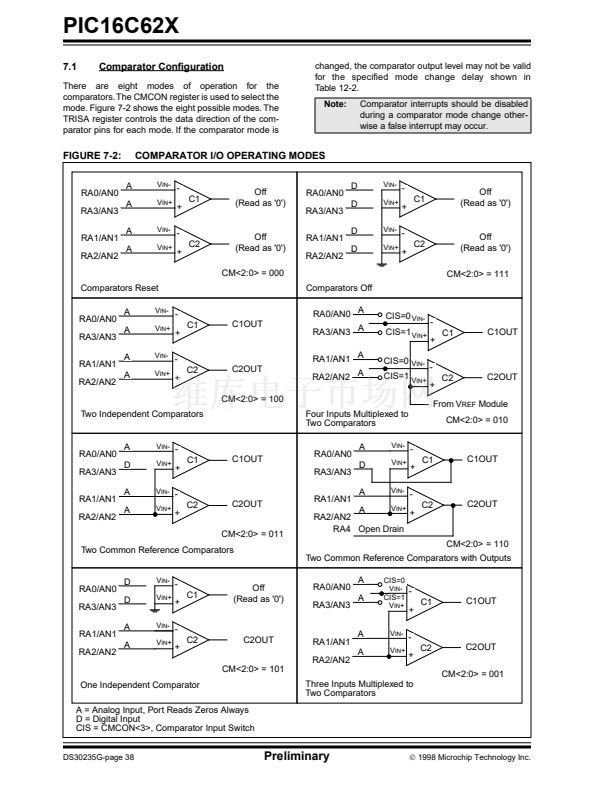
The Voltage Reference can output 16 distinct voltage
levels for each range.
The equations used to calculate the output of the
Voltage Reference are as follows:
if V
RR
= 1: V
REF
= (V
R
<3:0>/24) x V
DD
if V
RR
= 0: V
REF
= (V
DD
x 1/4) + (V
R
<3:0>/32) x V
DD
The setting time of the Voltage Reference must be
considered when changing the V
REF
output
(Table 12-2). Example 8-1 shows an example of how to
con铿乬ure the Voltage Reference for an output voltage
of 1.25V with V
DD
= 5.0V.
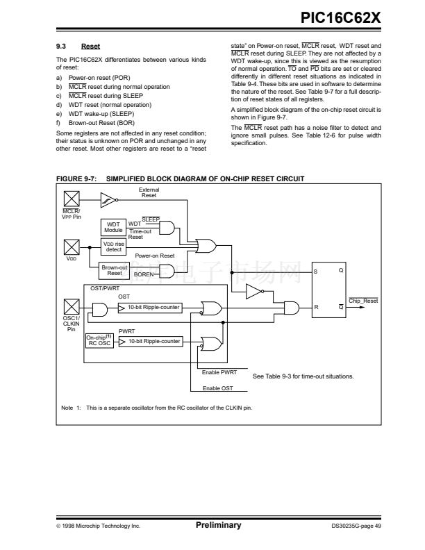
The Voltage Reference is a 16-tap resistor ladder
network that provides a selectable voltage reference.
The resistor ladder is segmented to provide two ranges
of V
REF
values and has a power-down function to
conserve power when the reference is not being used.
The VRCON register controls the operation of the
reference as shown in Figure 8-1. The block diagram is
given in Figure 8-2.
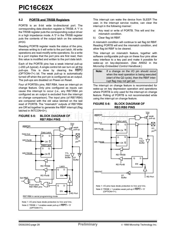
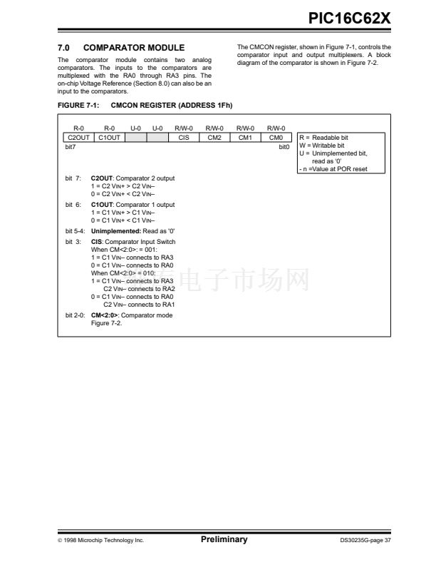
FIGURE 8-1:
R/W-0
V
REN
bit7
VRCON REGISTER(ADDRESS 9Fh)
R/W-0
V
RR
U-0
鈥?/div>
R/W-0
V
R3
R/W-0
V
R2
R/W-0
V
R1
R/W-0
V
R0
bit0
R/W-0
V
ROE
R = Readable bit
W = Writable bit
U = Unimplemented bit,
read as 鈥?鈥?/div>
- n =Value at POR reset
bit 7:
V
REN
:
V
REF
Enable
1 = V
REF
circuit powered on
0 = V
REF
circuit powered down, no I
DD
drain
V
ROE
:
V
REF
Output Enable
1 = V
REF
is output on RA2 pin
0 = V
REF
is disconnected from RA2 pin
V
RR
:
V
REF
Range selection
1 = Low Range
0 = High Range
Unimplemented:
Read as '0'
bit 6:
bit 5:
bit 4:
bit 3-0:
V
R
<3:0>:
V
REF
value selection 0
鈮?/div>
V
R
[3:0]
鈮?/div>
15
when V
RR
= 1: V
REF
= (V
R
<3:0>/ 24) * V
DD
when V
RR
= 0: V
REF
= 1/4 * V
DD
+ (V
R
<3:0>/ 32) * V
DD
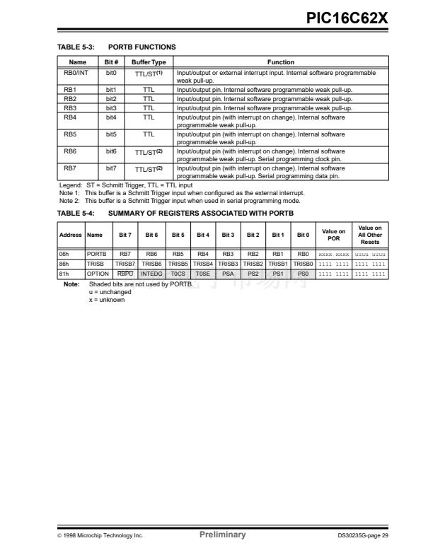
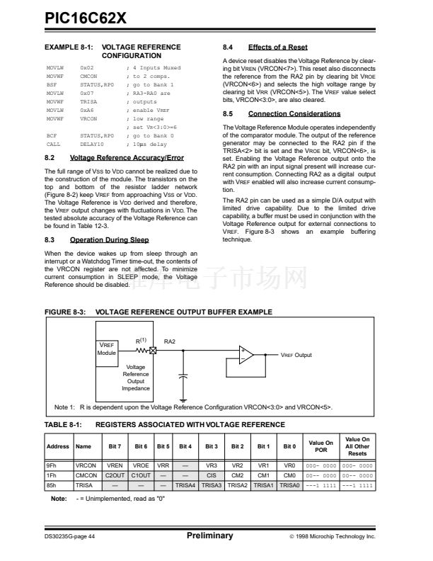
FIGURE 8-2:
VOLTAGE REFERENCE BLOCK DIAGRAM
16 Stages
V
REN
8R
R
R
R
R
8R
V
RR
V
R
3
V
REF
16-1 Analog Mux
V
R
0
(From VRCON<3:0>)
Note:
R is de铿乶ed in Table 12-3.
漏
1998 Microchip Technology Inc.
Preliminary
DS30235G-page 43


 1
1
 2
2
 3
3
 4
4
 5
5
 6
6
 7
7
 8
8
 9
9
 10
10
 11
11
 12
12
 13
13
 14
14
 15
15
 16
16
 17
17
 18
18
 19
19
 20
20
 21
21
 22
22
 23
23
 24
24
 25
25
 26
26
 27
27
 28
28
 29
29
 30
30
 31
31
 32
32
 33
33
 34
34
 35
35
 36
36
 37
37
 38
38
 39
39
 40
40
 41
41
 42
42
 43
43
 44
44
 45
45
 46
46
 47
47
 48
48
 49
49
 50
50
 51
51
 52
52
 53
53
 54
54
 55
55
 56
56
 57
57
 58
58
 59
59
 60
60
 61
61
 62
62
 63
63
 64
64
 65
65
 66
66
 67
67
 68
68
 69
69
 70
70
 71
71
 72
72
 73
73
 74
74
 75
75
 76
76
 77
77
 78
78
 79
79
 80
80
 81
81
 82
82
 83
83
 84
84
 85
85
 86
86
 87
87
 88
88
 89
89
 90
90
 91
91
 92
92
 93
93
 94
94
 95
95
 96
96
 97
97
 98
98
 99
99
 100
100
 101
101
 102
102
 103
103
 104
104
 105
105
 106
106
 107
107
 108
108
