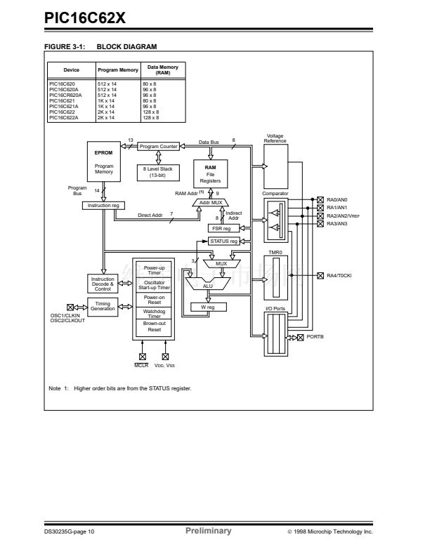
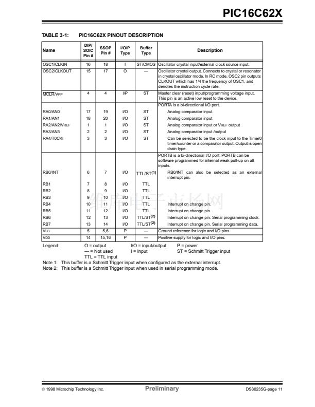
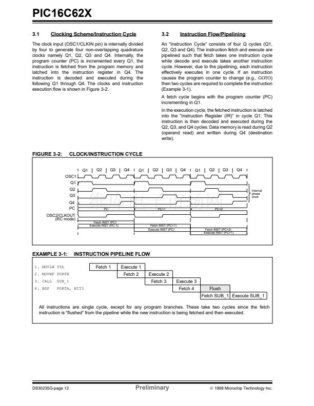
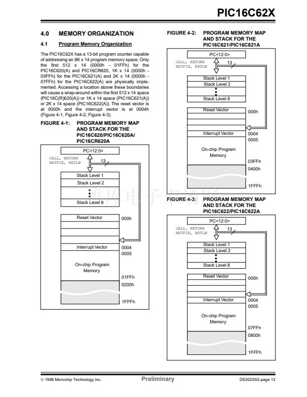
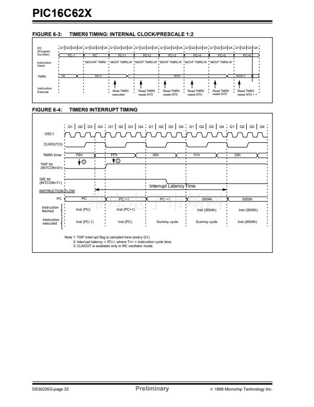
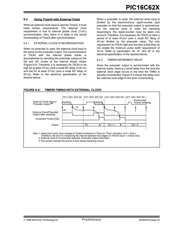
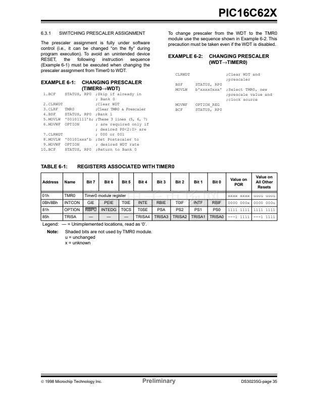
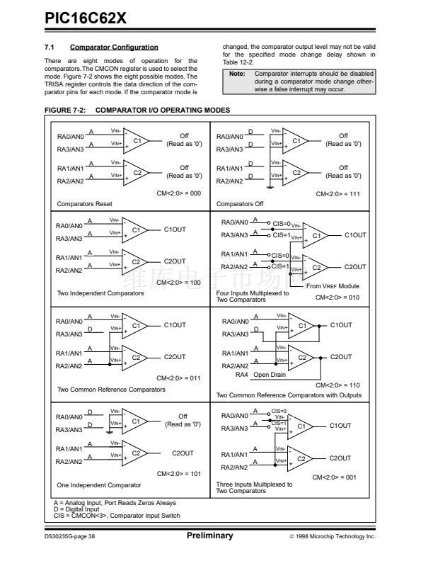
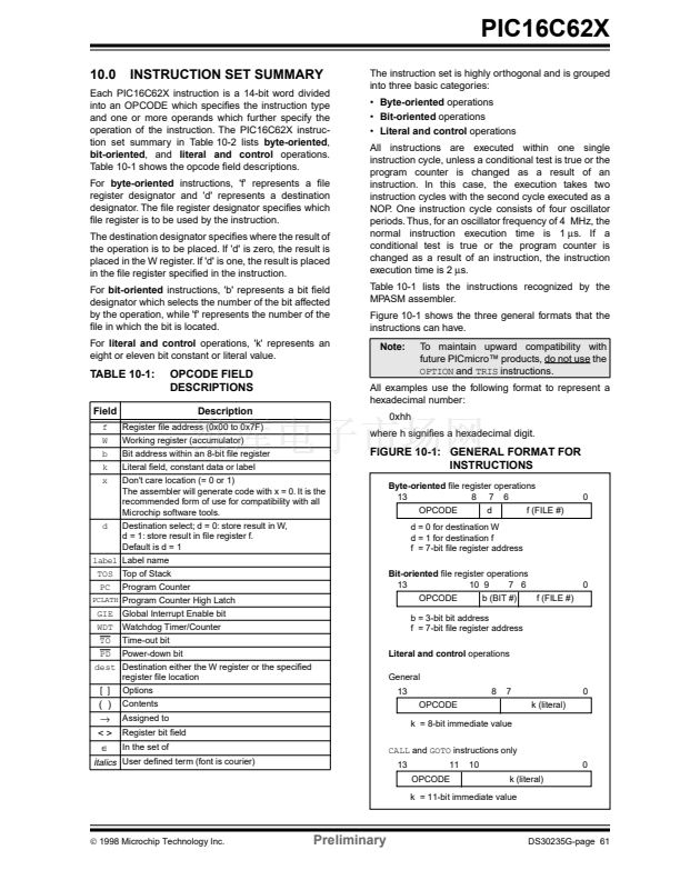
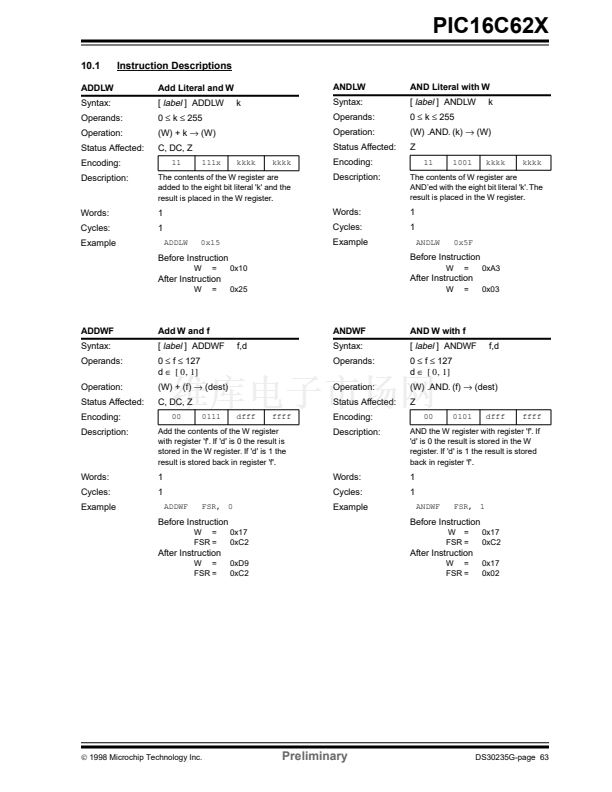
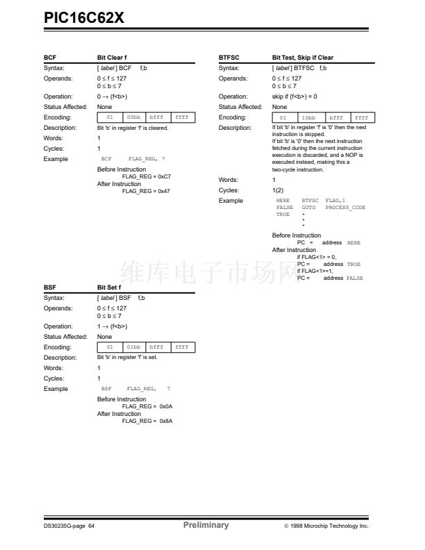
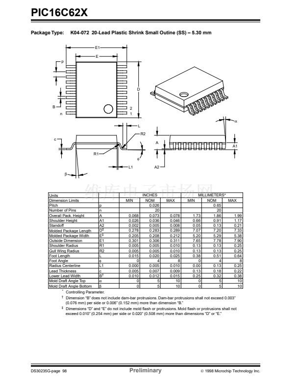
PIC16C62X
9.5.1
RB0/INT INTERRUPT
9.5.3
PORTB INTERRUPT
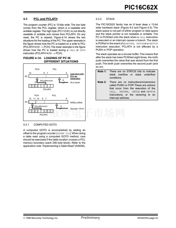
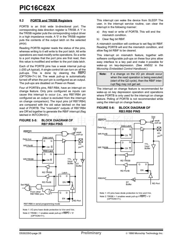
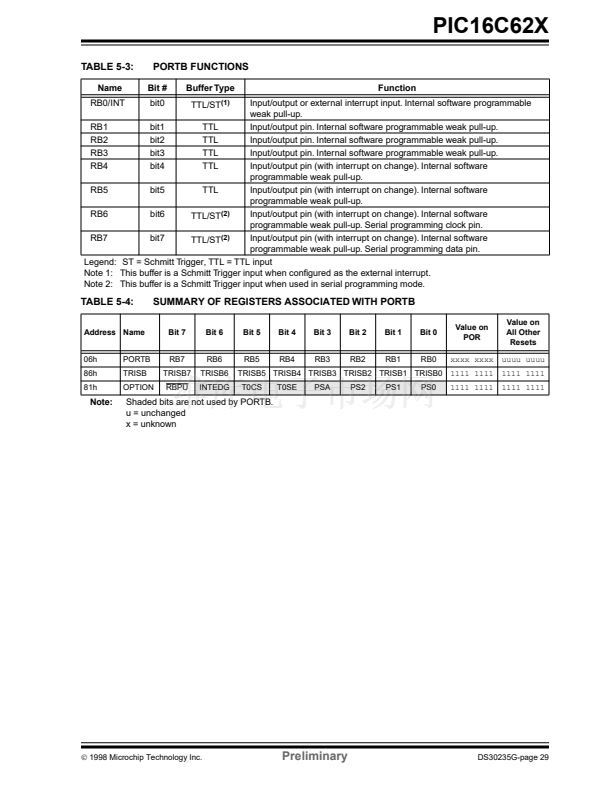
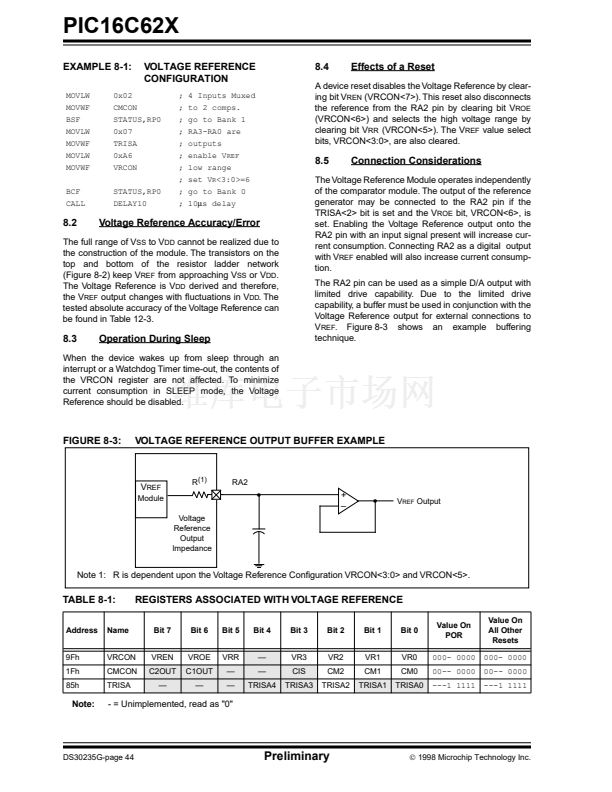
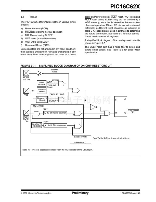
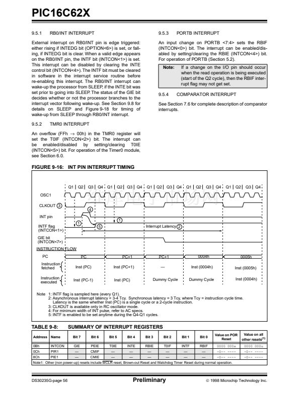
External interrupt on RB0/INT pin is edge triggered:
either rising if INTEDG bit (OPTION<6>) is set, or fall-
ing, if INTEDG bit is clear. When a valid edge appears
on the RB0/INT pin, the INTF bit (INTCON<1>) is set.
This interrupt can be disabled by clearing the INTE
control bit (INTCON<4>). The INTF bit must be cleared
in software in the interrupt service routine before
re-enabling this interrupt. The RB0/INT interrupt can
wake-up the processor from SLEEP, if the INTE bit was
set prior to going into SLEEP. The status of the GIE bit
decides whether or not the processor branches to the
interrupt vector following wake-up. See Section 9.8 for
details on SLEEP and Figure 9-18 for timing of
wake-up from SLEEP through RB0/INT interrupt.
9.5.2
TMR0 INTERRUPT
An input change on PORTB <7:4> sets the RBIF
(INTCON<0>) bit. The interrupt can be enabled/dis-
abled by setting/clearing the RBIE (INTCON<4>) bit.
For operation of PORTB (Section 5.2).
Note:
If a change on the I/O pin should occur
when the read operation is being executed
(start of the Q2 cycle), then the RBIF inter-
rupt 铿俛g may not get set.
COMPARATOR INTERRUPT
9.5.4
See Section 7.6 for complete description of comparator
interrupts.
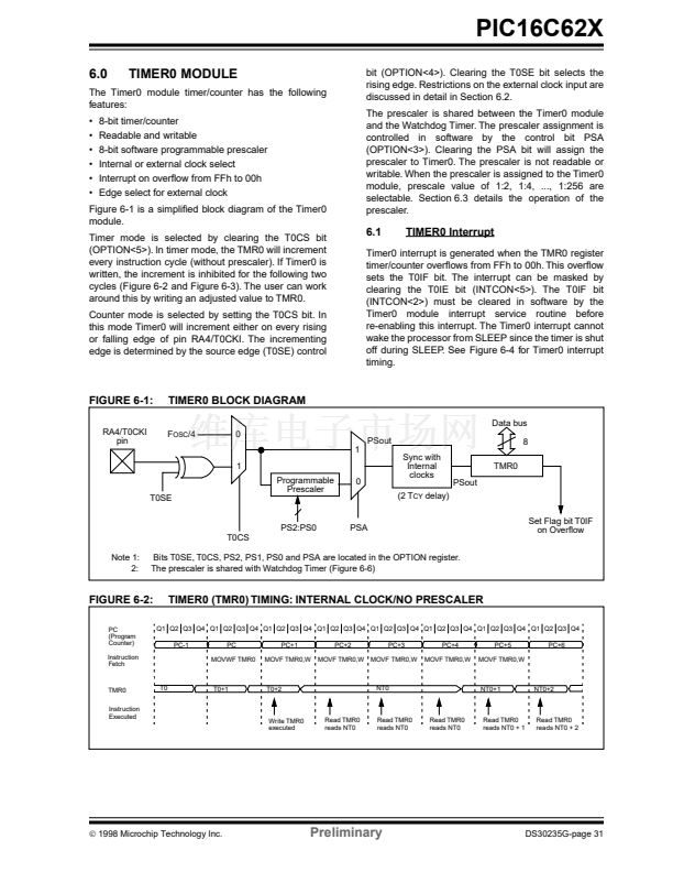
An over铿俹w (FFh
鈫?/div>
00h) in the TMR0 register will
set the T0IF (INTCON<2>) bit. The interrupt can
be enabled/disabled by setting/clearing T0IE
(INTCON<5>) bit. For operation of the Timer0 module,
see Section 6.0.
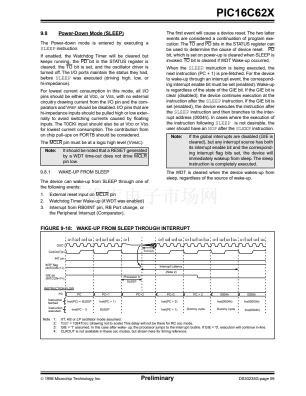
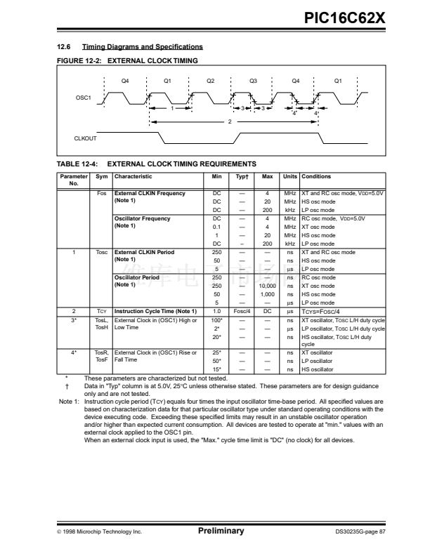
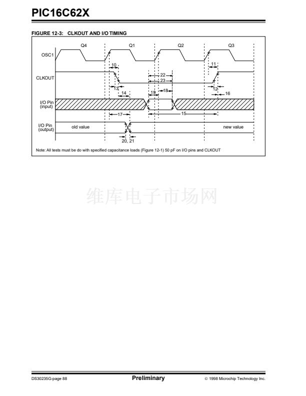
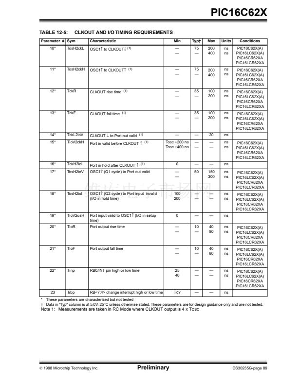
FIGURE 9-16: INT PIN INTERRUPT TIMING
Q1
OSC1
CLKOUT 3
INT pin
INTF 铿俛g
(INTCON<1>)
GIE bit
(INTCON<7>)
INSTRUCTION FLOW
PC
Instruction
fetched
Instruction
executed
Q2
Q3
Q4
Q1
Q2
Q3
Q4
Q1
Q2
Q3
Q4
Q1
Q2
Q3
Q4
Q1
Q2
Q3
Q4
4
1
5
Interrupt Latency 2
1
PC
Inst (PC)
Inst (PC-1)
PC+1
Inst (PC+1)
Inst (PC)
PC+1
鈥?/div>
Dummy Cycle
0004h
Inst (0004h)
Dummy Cycle
0005h
Inst (0005h)
Inst (0004h)
Note 1: INTF 铿俛g is sampled here (every Q1).
2: Asynchronous interrupt latency = 3-4 Tcy. Synchronous latency = 3 Tcy, where Tcy = instruction cycle time.
Latency is the same whether Inst (PC) is a single cycle or a 2-cycle instruction.
3: CLKOUT is available only in RC oscillator mode.
4: For minimum width of INT pulse, refer to AC specs.
5: INTF is enabled to be set anytime during the Q4-Q1 cycles.
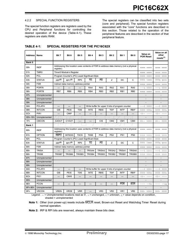
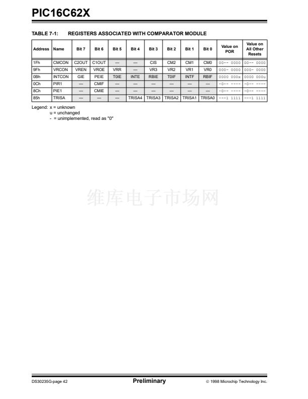
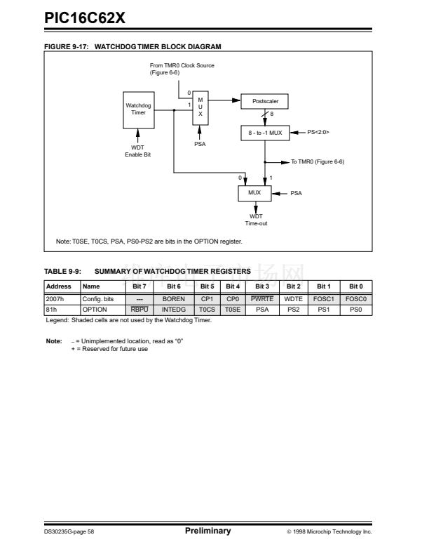
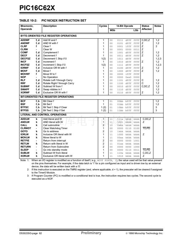
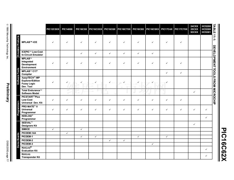
TABLE 9-8:
Address
0Bh
0Ch
8Ch
Name
INTCON
PIR1
PIE1
SUMMARY OF INTERRUPT REGISTERS
Bit 7
GIE
鈥?/div>
鈥?/div>
Bit 6
PEIE
CMIF
CMIE
Bit 5
T0IE
鈥?/div>
鈥?/div>
Bit 4
INTE
鈥?/div>
鈥?/div>
Bit 3
RBIE
鈥?/div>
鈥?/div>
Bit 2
T0IF
鈥?/div>
鈥?/div>
Bit 1
INTF
鈥?/div>
鈥?/div>
Bit 0
RBIF
鈥?/div>
鈥?/div>
Value on POR
Reset
0000 000x
-0-- ----
-0-- ----
Value on all
other resets
(1)
0000 000u
-0-- ----
-0-- ----
Note1: Other (non power-up) resets include MCLR reset, Brown-out Reset and Watchdog Timer Reset during normal operation.
DS30235G-page 56
Preliminary
漏
1998 Microchip Technology Inc.
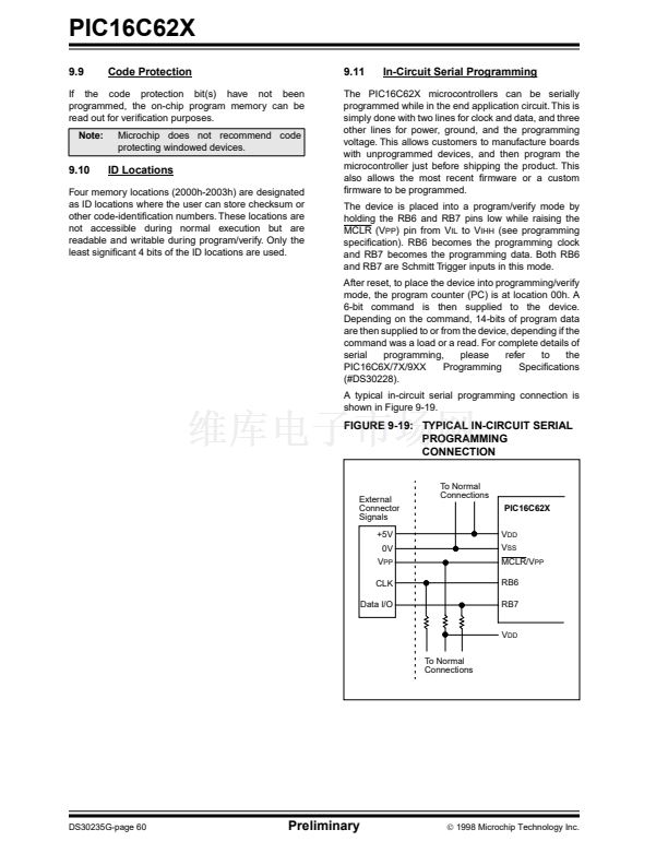
PIC16C621A相关型号PDF文件下载
-
型号
版本
描述
厂商
下载
-
英文版
8-Pin FLASH-Based 8-Bit CMOS Microcontrollers
-
英文版
8-Pin, 8-Bit CMOS Microcontroller with EEPROM Data Memory
MICROCHIP ...
-
英文版
8-Pin, 8-Bit CMOS Microcontroller with A/D Converter and EEP...
MICROCHIP ...
-
英文版
8-Pin, 8-Bit CMOS Microcontrollers
MICROCHIP ...
-
英文版
EPROM Memory Programming Specification
MICROCHIP ...
-
英文版
8-Pin FLASH-Based 8-Bit CMOS Microcontrollers
MICROCHIP ...
-
英文版
Microcontroller
-
英文版
Microcontroller
-
英文版
Microcontroller
ETC
-
英文版
EPROM-Based 8-Bit CMOS Microcontroller
-
英文版
8-Pin, 8-Bit CMOS Microcontrollers
-
英文版
8-Pin, 8-Bit CMOS Microcontrollers
MICROCHIP ...
-
英文版
ETC
-
英文版
EPROM Memory Programming Specification
-
英文版
EPROM Memory Programming Specification
MICROCHIP ...
-
英文版
28-Pin Programmable Mixed Signal Controller
-
英文版
EPROM Memory Programming Specification
-
英文版
Microcontroller
ETC
-
英文版
Microcontroller
ETC
-
英文版
EPROM/ROM-Based 8-Bit CMOS Microcontroller Series


 1
1
 2
2
 3
3
 4
4
 5
5
 6
6
 7
7
 8
8
 9
9
 10
10
 11
11
 12
12
 13
13
 14
14
 15
15
 16
16
 17
17
 18
18
 19
19
 20
20
 21
21
 22
22
 23
23
 24
24
 25
25
 26
26
 27
27
 28
28
 29
29
 30
30
 31
31
 32
32
 33
33
 34
34
 35
35
 36
36
 37
37
 38
38
 39
39
 40
40
 41
41
 42
42
 43
43
 44
44
 45
45
 46
46
 47
47
 48
48
 49
49
 50
50
 51
51
 52
52
 53
53
 54
54
 55
55
 56
56
 57
57
 58
58
 59
59
 60
60
 61
61
 62
62
 63
63
 64
64
 65
65
 66
66
 67
67
 68
68
 69
69
 70
70
 71
71
 72
72
 73
73
 74
74
 75
75
 76
76
 77
77
 78
78
 79
79
 80
80
 81
81
 82
82
 83
83
 84
84
 85
85
 86
86
 87
87
 88
88
 89
89
 90
90
 91
91
 92
92
 93
93
 94
94
 95
95
 96
96
 97
97
 98
98
 99
99
 100
100
 101
101
 102
102
 103
103
 104
104
 105
105
 106
106
 107
107
 108
108
