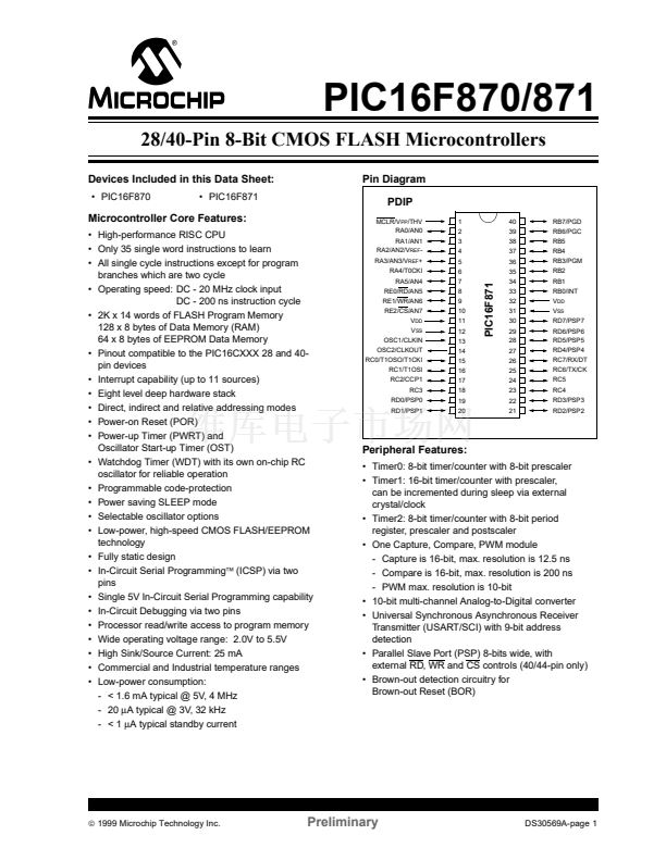
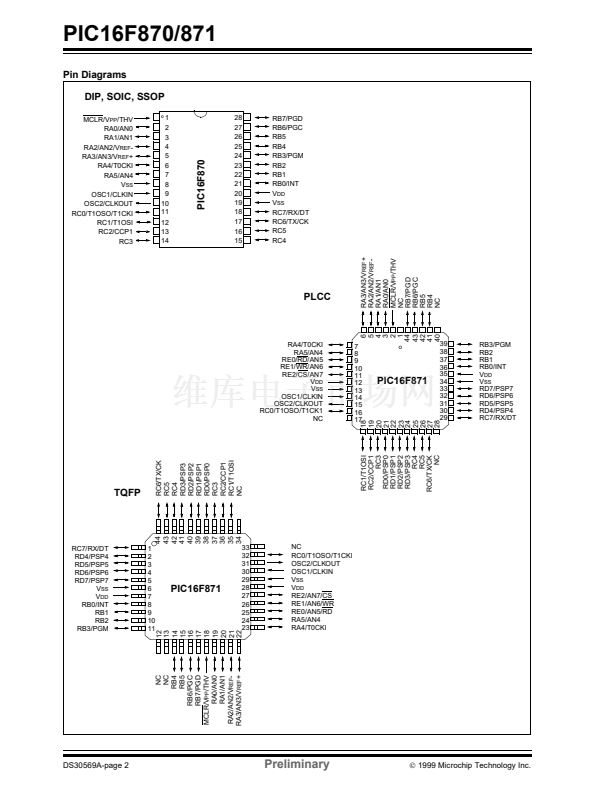
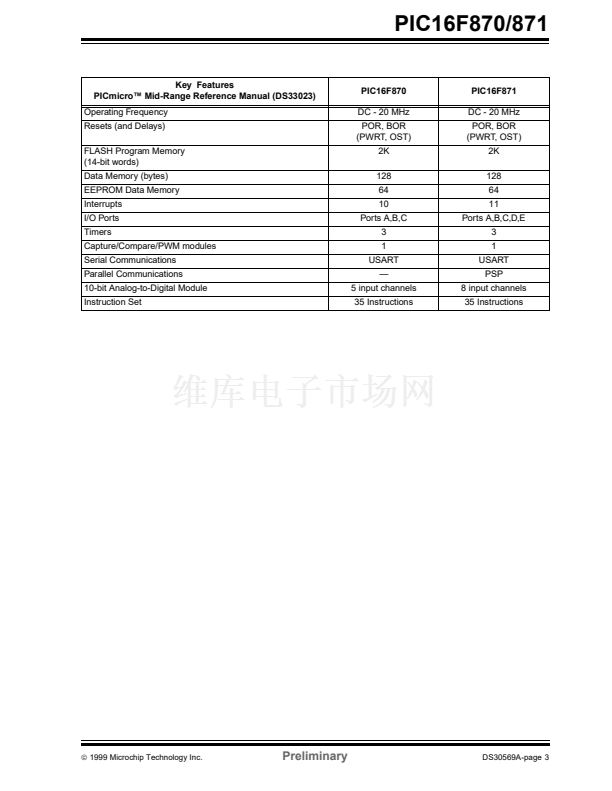
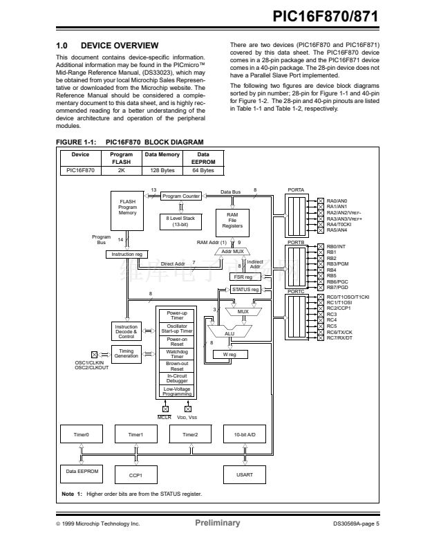
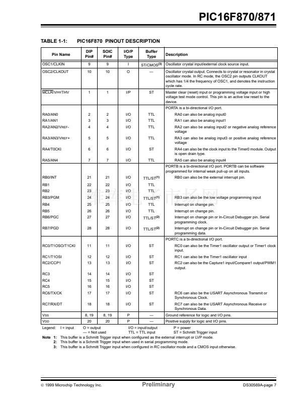
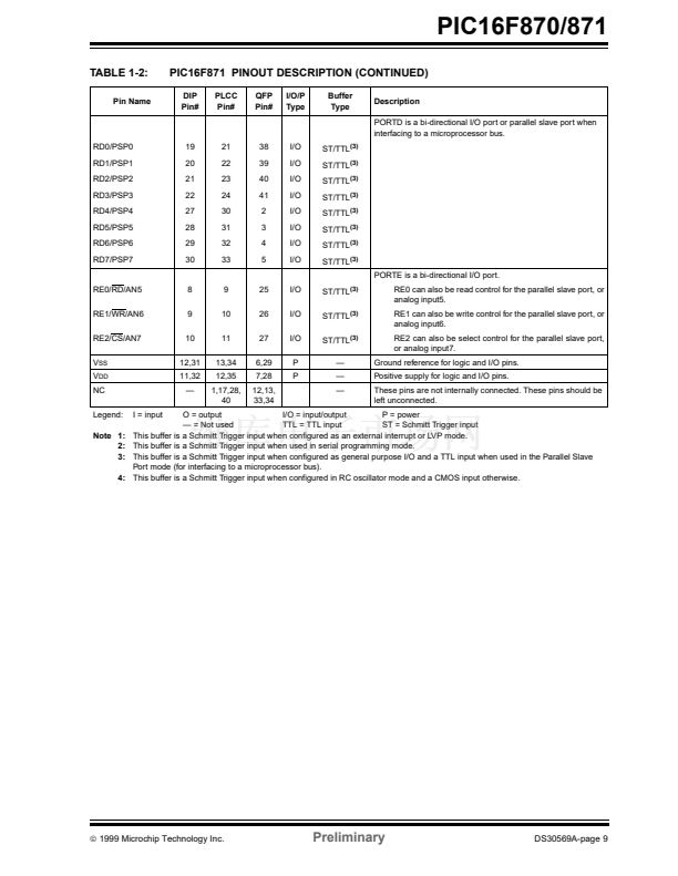
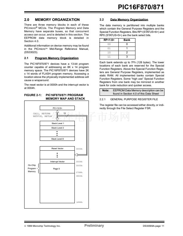
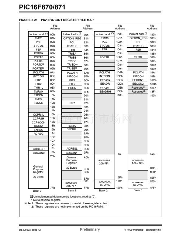
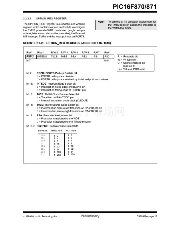
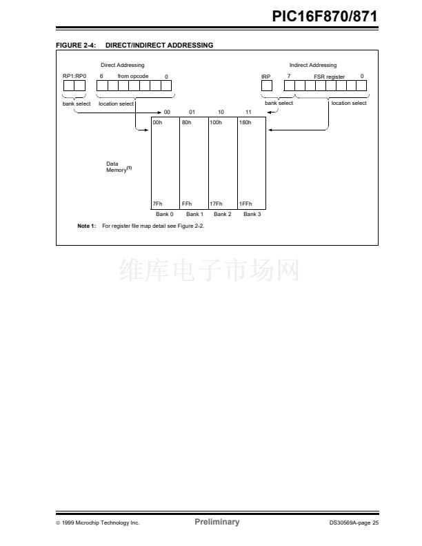
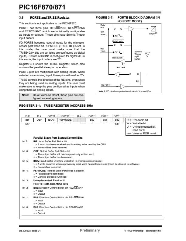
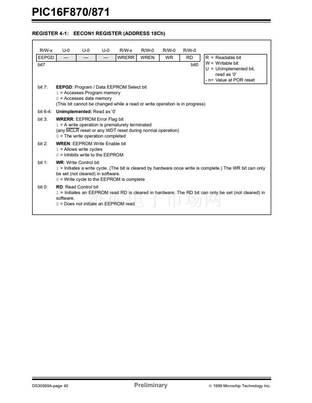
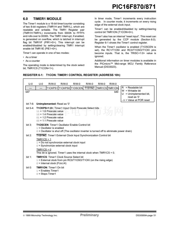
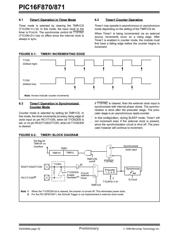
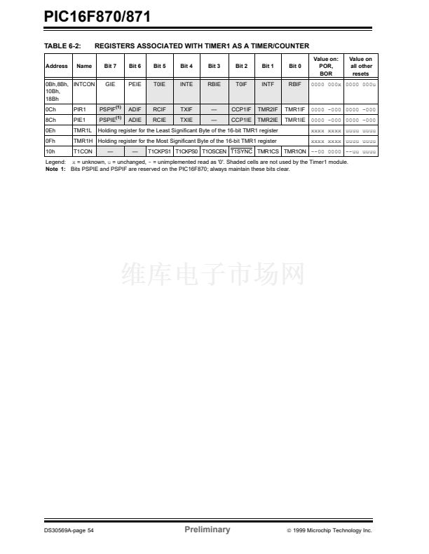
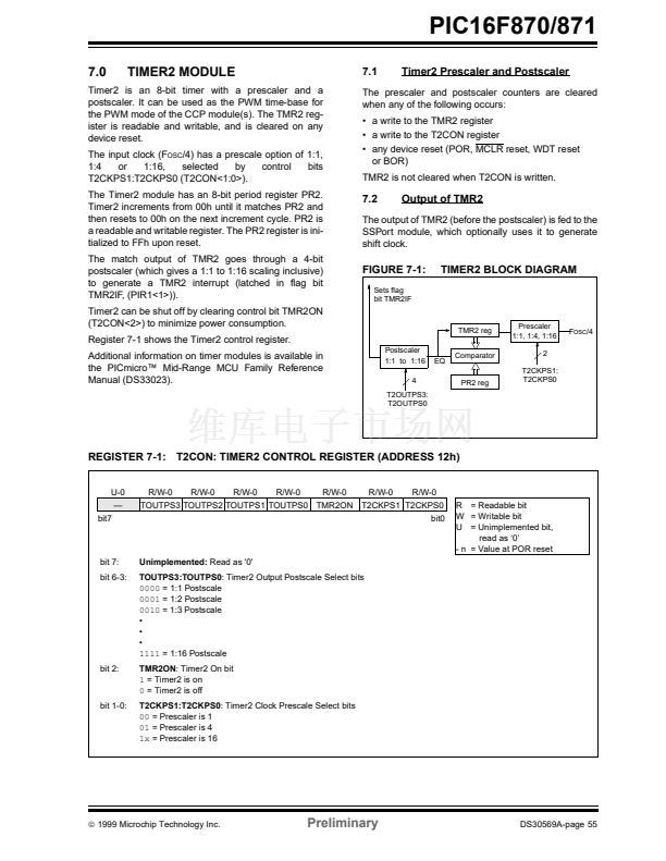
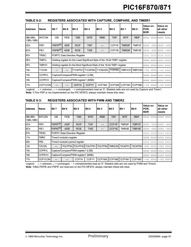
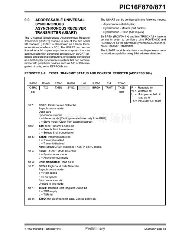
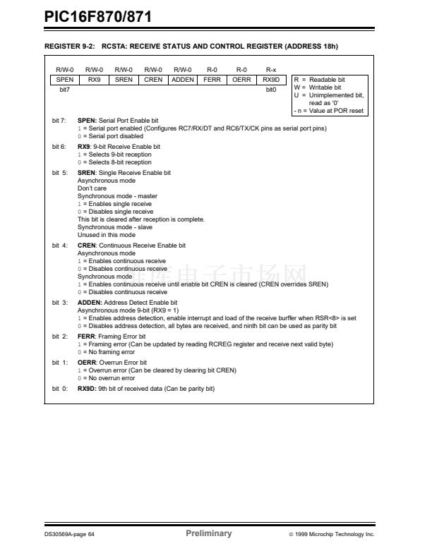
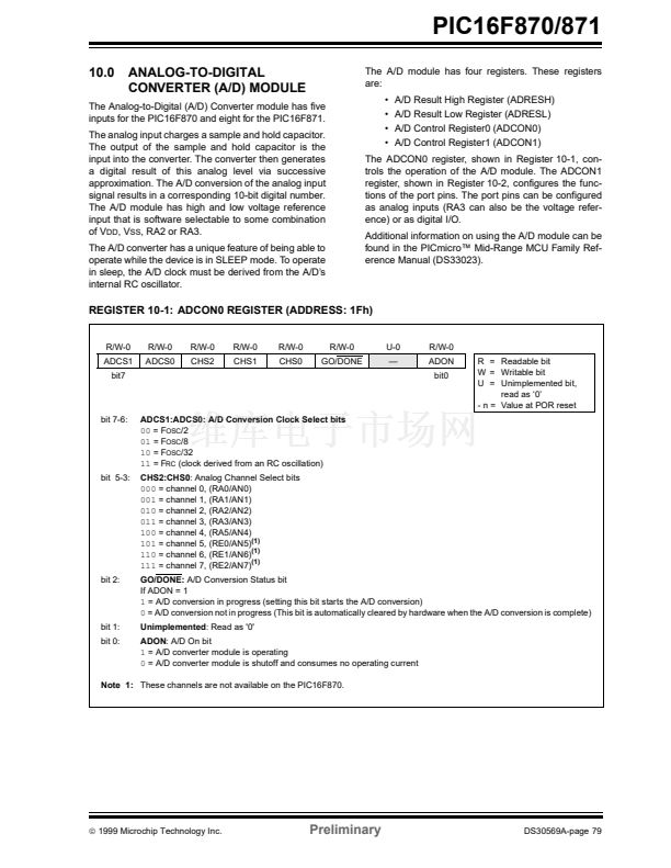
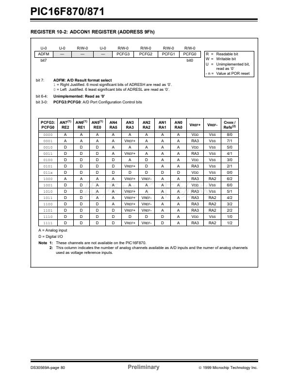
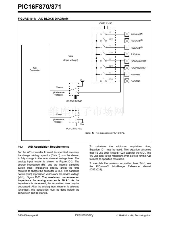
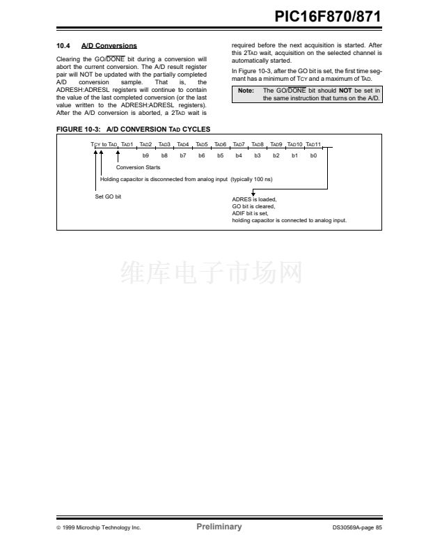
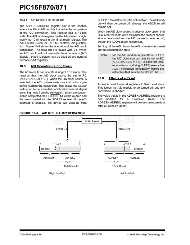
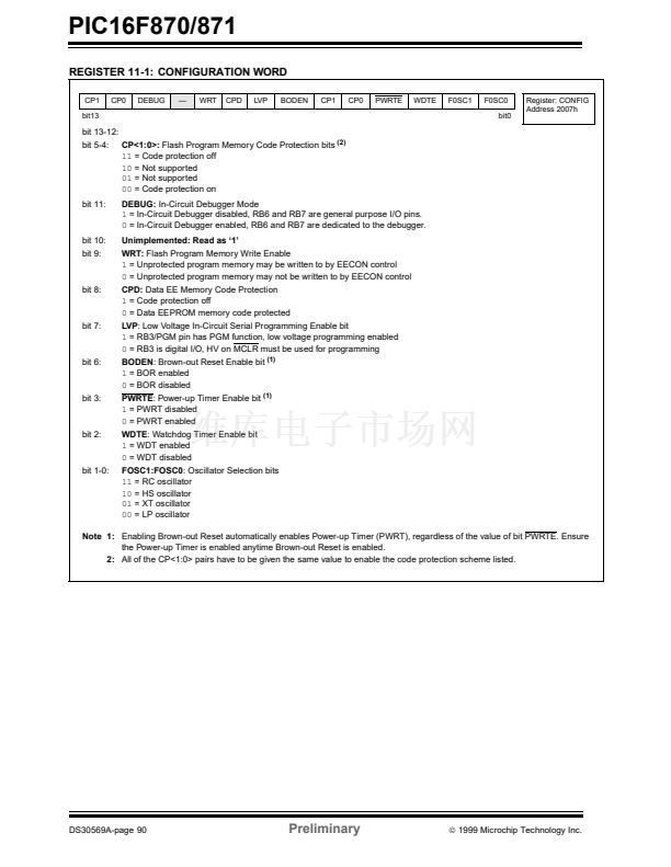
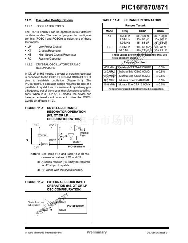
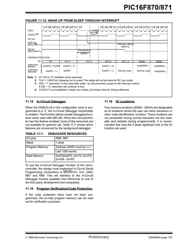
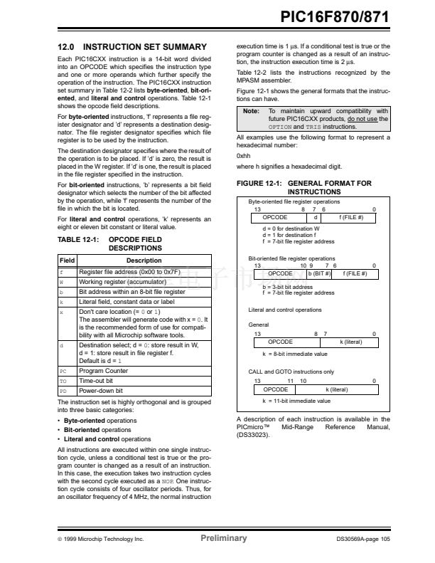
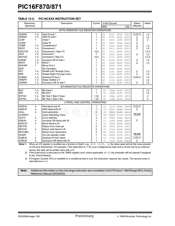
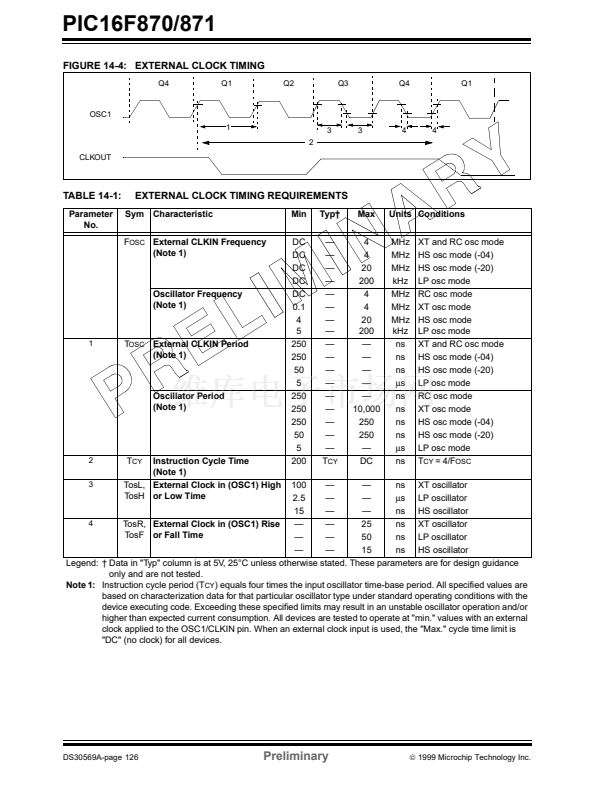
PIC16F870/871
9.3.2
USART SYNCHRONOUS MASTER
RECEPTION
Once synchronous mode is selected, reception is
enabled by setting either enable bit SREN (RCSTA<5>)
or enable bit CREN (RCSTA<4>). Data is sampled on
the RC7/RX/DT pin on the falling edge of the clock. If
enable bit SREN is set, then only a single word is
received. If enable bit CREN is set, the reception is
continuous until CREN is cleared. If both bits are set,
CREN takes precedence. After clocking the last bit, the
received data in the Receive Shift Register (RSR) is
transferred to the RCREG register (if it is empty). When
the transfer is complete, interrupt flag bit RCIF
(PIR1<5>) is set. The actual interrupt can be enabled/
disabled by setting/clearing enable bit RCIE (PIE1<5>).
Flag bit RCIF is a read only bit, which is reset by the
hardware. In this case, it is reset when the RCREG reg-
ister has been read and is empty. The RCREG is a dou-
ble buffered register (i.e., it is a two deep FIFO). It is
possible for two bytes of data to be received and trans-
ferred to the RCREG FIFO and a third byte to begin
shifting into the RSR register. On the clocking of the last
bit of the third byte, if the RCREG register is still full,
then overrun error bit OERR (RCSTA<1>) is set. The
word in the RSR will be lost. The RCREG register can
be read twice to retrieve the two bytes in the FIFO. Bit
OERR has to be cleared in software (by clearing bit
CREN). If bit OERR is set, transfers from the RSR to
the RCREG are inhibited, so it is essential to clear bit
OERR if it is set. The ninth receive bit is buffered the
same way as the receive data. Reading the RCREG
register will load bit RX9D with a new value, therefore it
is essential for the user to read the RCSTA register
before reading RCREG in order not to lose the old
RX9D information.
Steps to follow when setting up a Synchronous Master
Reception:
1.
Initialize the SPBRG register for the appropriate
baud rate. (Section 9.1)
2. Enable the synchronous master serial port by
setting bits SYNC, SPEN and CSRC.
3. Ensure bits CREN and SREN are clear.
4. If interrupts are desired, then set enable bit RCIE.
5. If 9-bit reception is desired, then set bit RX9.
6. If a single reception is required, set bit SREN.
For continuous reception set bit CREN.
7. Interrupt flag bit RCIF will be set when reception
is complete and an interrupt will be generated if
enable bit RCIE was set.
8. Read the RCSTA register to get the ninth bit (if
enabled) and determine if any error occurred
during reception.
9. Read the 8-bit received data by reading the
RCREG register.
10. If any error occurred, clear the error by clearing
bit CREN.
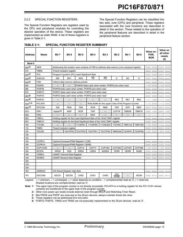
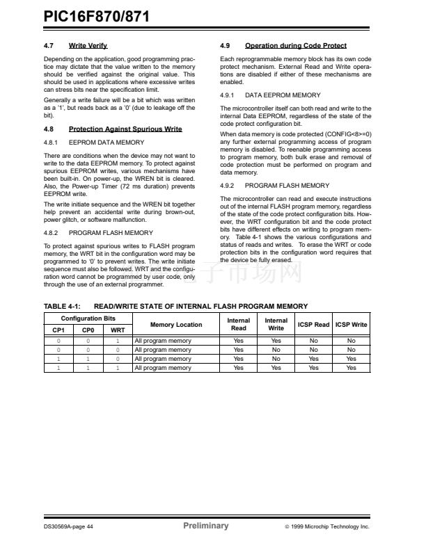
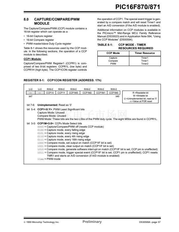
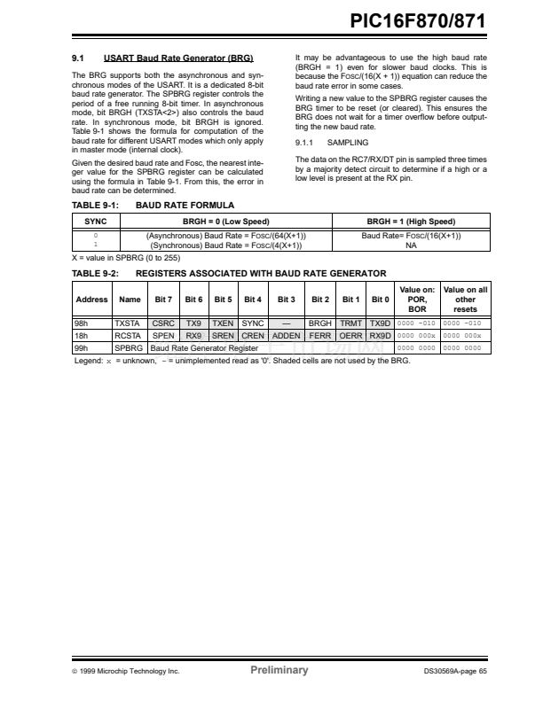
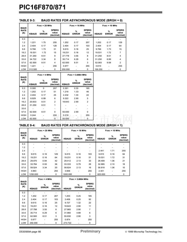
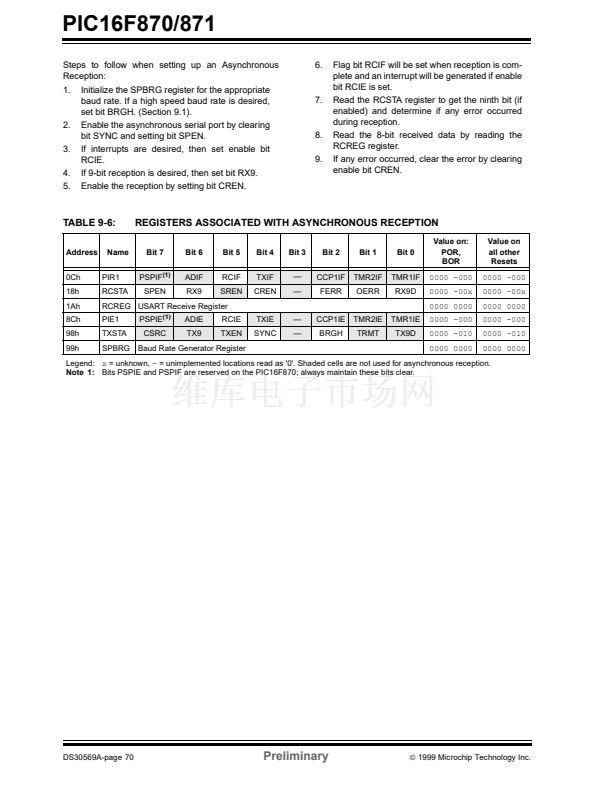
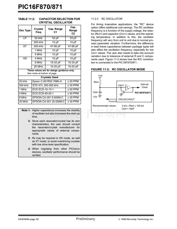
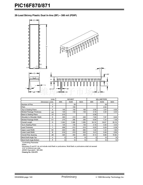
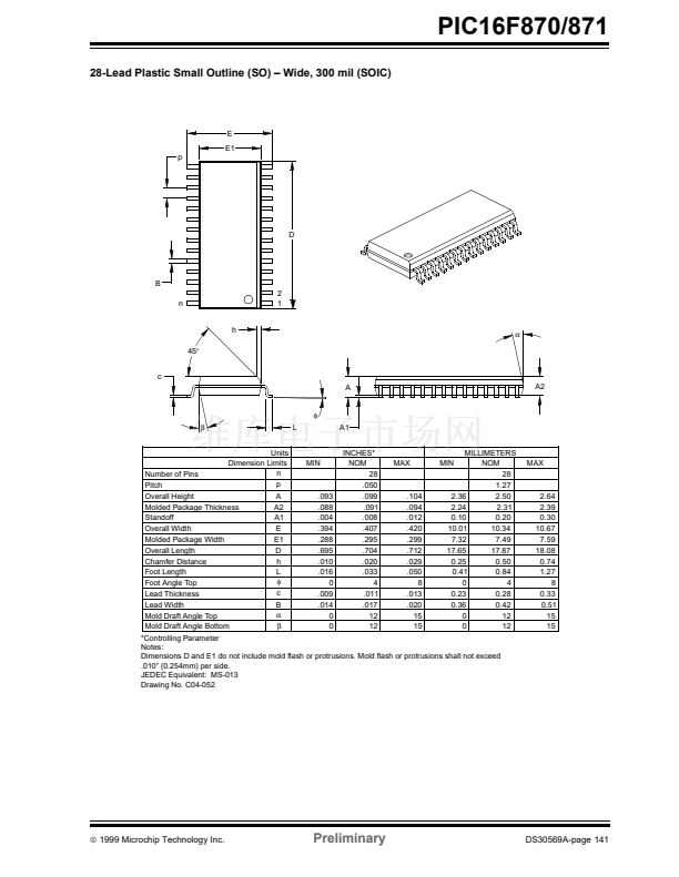
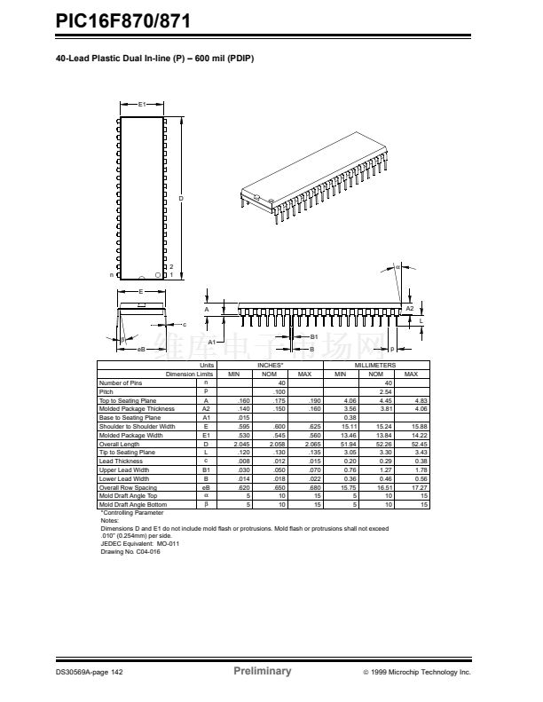
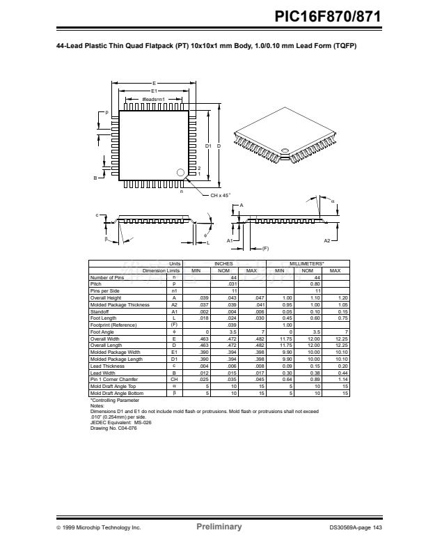
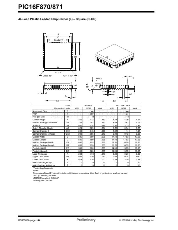
TABLE 9-9:
Address
0Ch
18h
1Ah
8Ch
98h
99h
Name
PIR1
RCSTA
RCREG
PIE1
TXSTA
SPBRG
REGISTERS ASSOCIATED WITH SYNCHRONOUS MASTER RECEPTION
Bit 7
PSPIF
(1)
SPEN
PSPIE
(1)
Bit 6
ADIF
RX9
ADIE
TX9
Bit 5
RCIF
SREN
RCIE
TXEN
Bit 4
TXIF
CREN
TXIE
SYNC
Bit 3
鈥?/div>
鈥?/div>
鈥?/div>
鈥?/div>
Bit 2
CCP1IF
FERR
CCP1IE
BRGH
Bit 1
TMR2IF
OERR
TMR2IE
TRMT
Bit 0
TMR1IF
RX9D
TMR1IE
TX9D
Value on:
POR,
BOR
0000 -000
0000 -00x
0000 0000
0000 -000
0000 -010
0000 0000
Value on all
other Resets
0000 -000
0000 -00x
0000 0000
0000 -000
0000 -010
0000 0000
USART Receive Register
CSRC
Baud Rate Generator Register
Legend:
x
= unknown,
-
= unimplemented read as '0'. Shaded cells are not used for synchronous master reception.
Note 1:
Bits PSPIE and PSPIF are reserved on the PIC16F870; always maintain these bits clear.
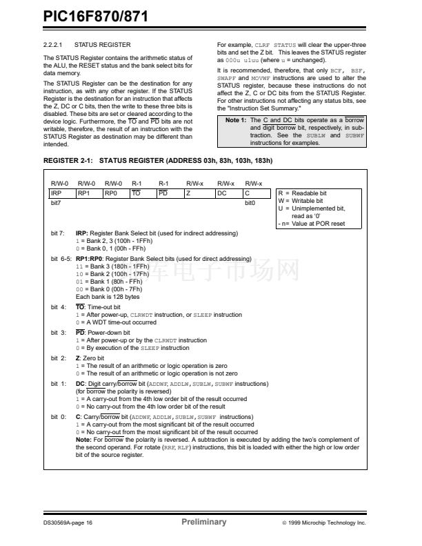
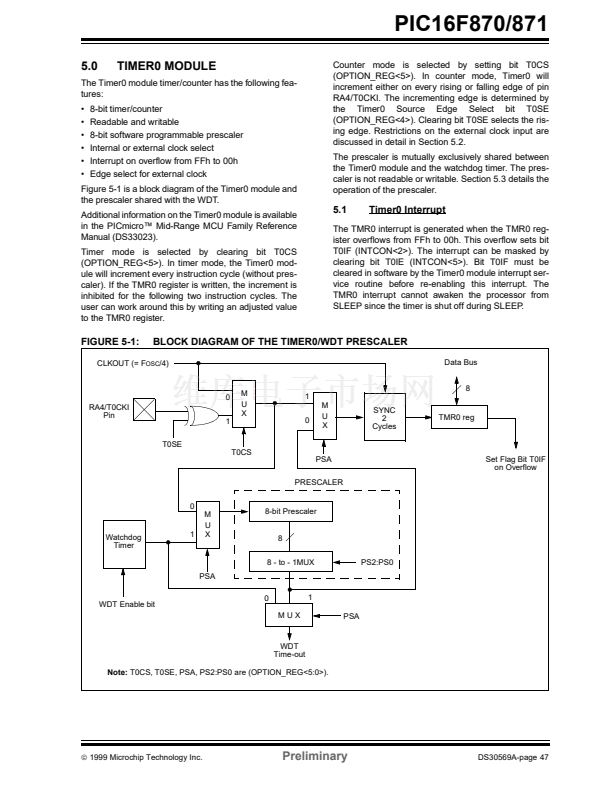
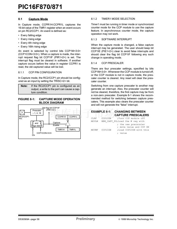
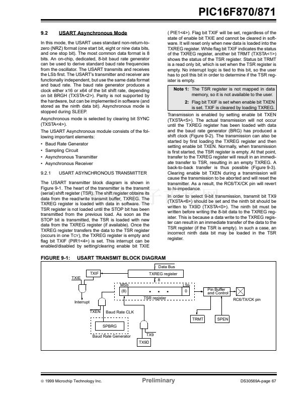
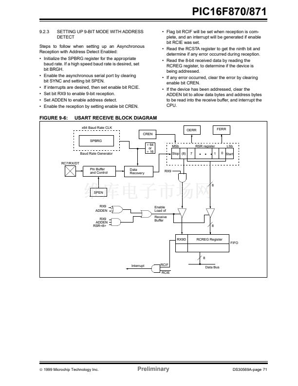
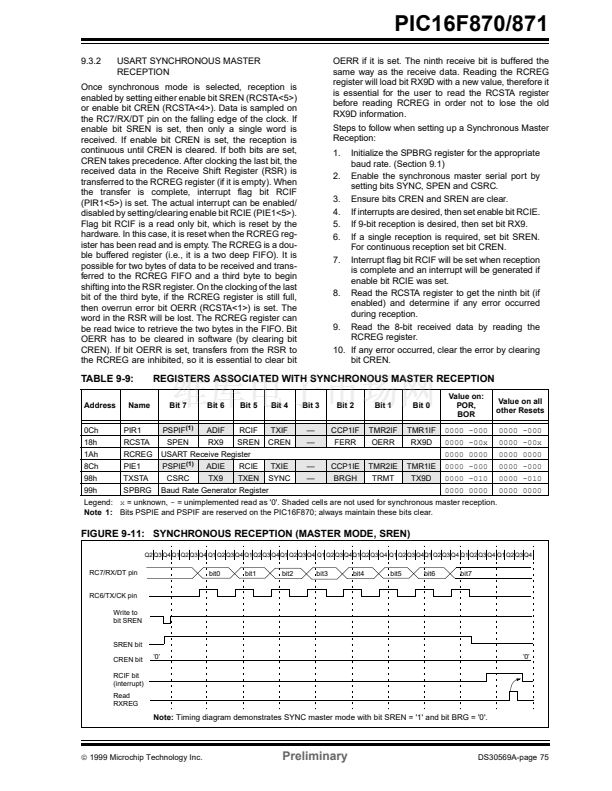
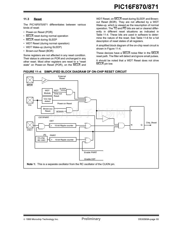
FIGURE 9-11: SYNCHRONOUS RECEPTION (MASTER MODE, SREN)
Q2 Q3 Q4 Q1 Q2 Q3 Q4 Q1 Q2 Q3 Q4 Q1 Q2 Q3 Q4Q1 Q2 Q3 Q4 Q1 Q2 Q3 Q4Q1 Q2 Q3 Q4 Q1 Q2 Q3 Q4Q1 Q2 Q3 Q4 Q1 Q2 Q3 Q4 Q1 Q2 Q3 Q4
RC7/RX/DT pin
RC6/TX/CK pin
Write to
bit SREN
SREN bit
CREN bit
RCIF bit
(interrupt)
Read
RXREG
鈥?鈥?/div>
bit0
bit1
bit2
bit3
bit4
bit5
bit6
bit7
鈥?鈥?/div>
Note:
Timing diagram demonstrates SYNC master mode with bit SREN = '1' and bit BRG = '0'.
漏
1999 Microchip Technology Inc.
Preliminary
DS30569A-page 75
PIC16F871相关型号PDF文件下载
-
型号
版本
描述
厂商
下载
-
英文版
8-Pin FLASH-Based 8-Bit CMOS Microcontrollers
-
英文版
8-Pin, 8-Bit CMOS Microcontroller with EEPROM Data Memory
MICROCHIP ...
-
英文版
8-Pin, 8-Bit CMOS Microcontroller with A/D Converter and EEP...
MICROCHIP ...
-
英文版
8-Pin, 8-Bit CMOS Microcontrollers
MICROCHIP ...
-
英文版
EPROM Memory Programming Specification
MICROCHIP ...
-
英文版
8-Pin FLASH-Based 8-Bit CMOS Microcontrollers
MICROCHIP ...
-
英文版
Microcontroller
-
英文版
Microcontroller
-
英文版
Microcontroller
ETC
-
英文版
EPROM-Based 8-Bit CMOS Microcontroller
-
英文版
8-Pin, 8-Bit CMOS Microcontrollers
-
英文版
8-Pin, 8-Bit CMOS Microcontrollers
MICROCHIP ...
-
英文版
ETC
-
英文版
EPROM Memory Programming Specification
-
英文版
EPROM Memory Programming Specification
MICROCHIP ...
-
英文版
28-Pin Programmable Mixed Signal Controller
-
英文版
EPROM Memory Programming Specification
-
英文版
Microcontroller
ETC
-
英文版
Microcontroller
ETC
-
英文版
EPROM/ROM-Based 8-Bit CMOS Microcontroller Series


 1
1
 2
2
 3
3
 4
4
 5
5
 6
6
 7
7
 8
8
 9
9
 10
10
 11
11
 12
12
 13
13
 14
14
 15
15
 16
16
 17
17
 18
18
 19
19
 20
20
 21
21
 22
22
 23
23
 24
24
 25
25
 26
26
 27
27
 28
28
 29
29
 30
30
 31
31
 32
32
 33
33
 34
34
 35
35
 36
36
 37
37
 38
38
 39
39
 40
40
 41
41
 42
42
 43
43
 44
44
 45
45
 46
46
 47
47
 48
48
 49
49
 50
50
 51
51
 52
52
 53
53
 54
54
 55
55
 56
56
 57
57
 58
58
 59
59
 60
60
 61
61
 62
62
 63
63
 64
64
 65
65
 66
66
 67
67
 68
68
 69
69
 70
70
 71
71
 72
72
 73
73
 74
74
 75
75
 76
76
 77
77
 78
78
 79
79
 80
80
 81
81
 82
82
 83
83
 84
84
 85
85
 86
86
 87
87
 88
88
 89
89
 90
90
 91
91
 92
92
 93
93
 94
94
 95
95
 96
96
 97
97
 98
98
 99
99
 100
100
 101
101
 102
102
 103
103
 104
104
 105
105
 106
106
 107
107
 108
108
 109
109
 110
110
 111
111
 112
112
 113
113
 114
114
 115
115
 116
116
 117
117
 118
118
 119
119
 120
120
 121
121
 122
122
 123
123
 124
124
 125
125
 126
126
 127
127
 128
128
 129
129
 130
130
 131
131
 132
132
 133
133
 134
134
 135
135
 136
136
 137
137
 138
138
 139
139
 140
140
 141
141
 142
142
 143
143
 144
144
 145
145
 146
146
 147
147
 148
148
 149
149
 150
150
 151
151
 152
152
 153
153
 154
154
 155
155
 156
156
