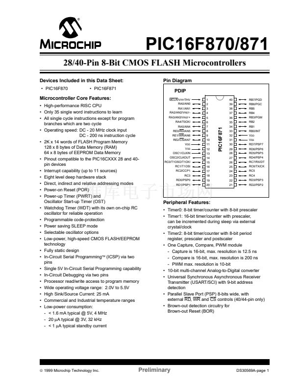
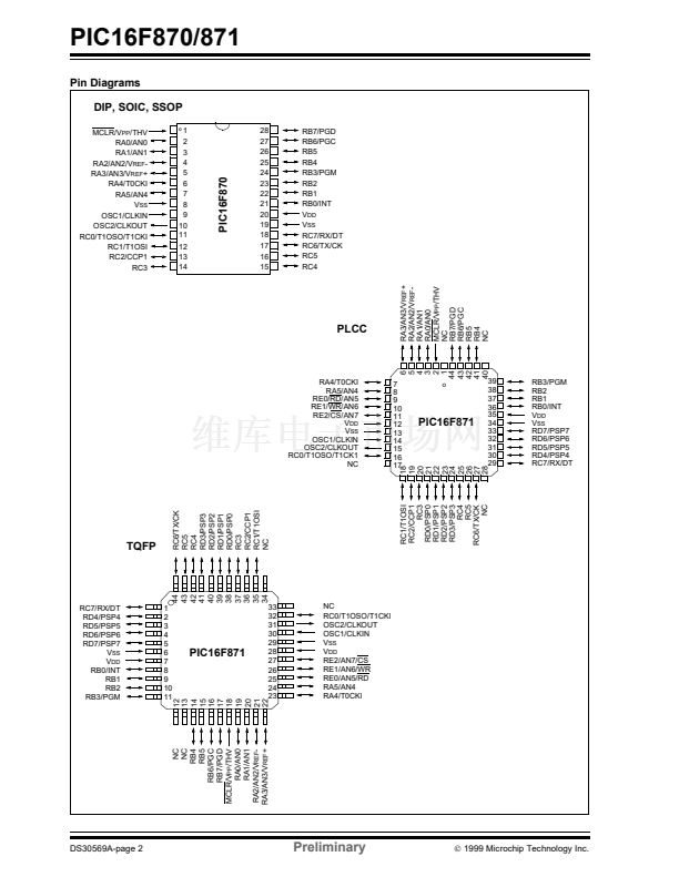
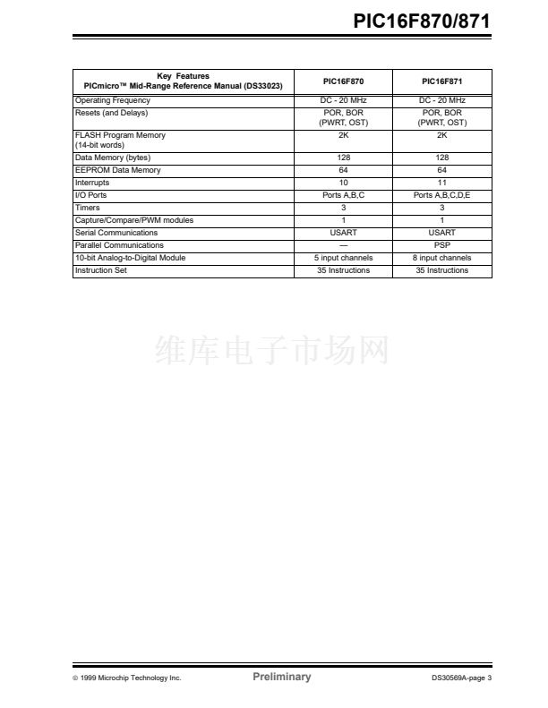
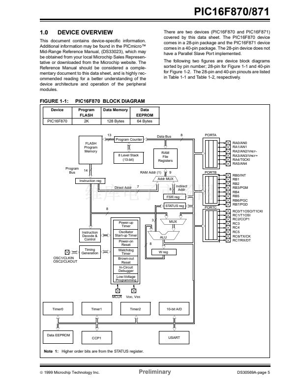
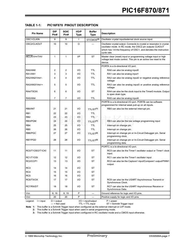
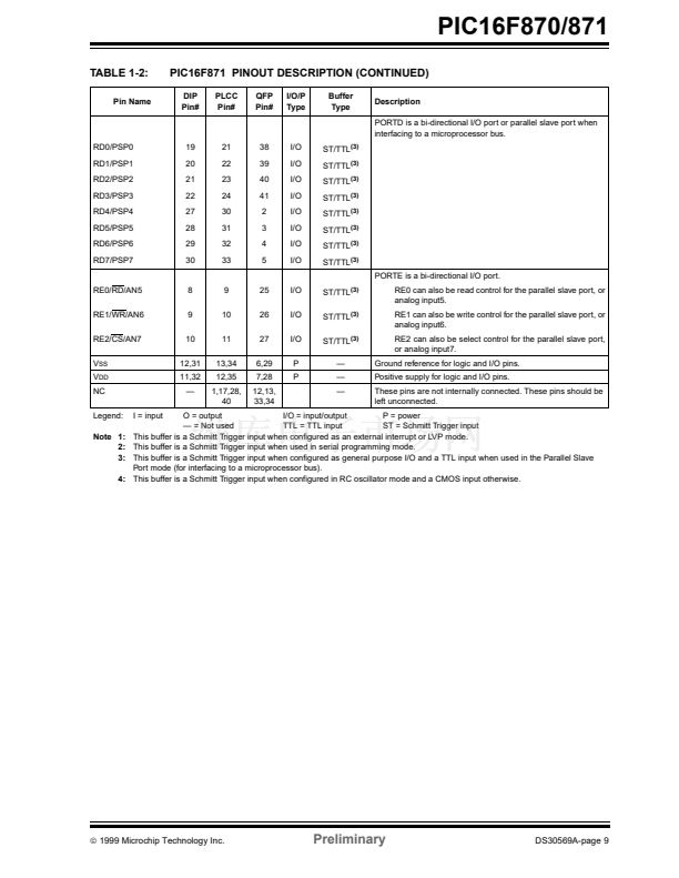
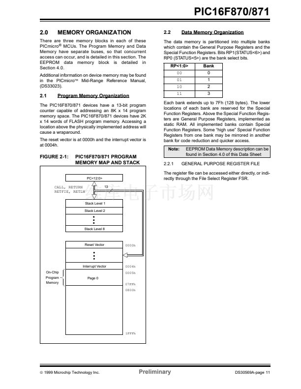
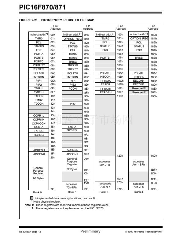
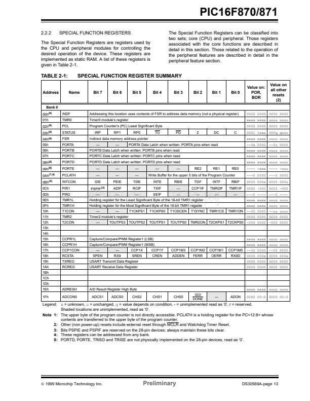
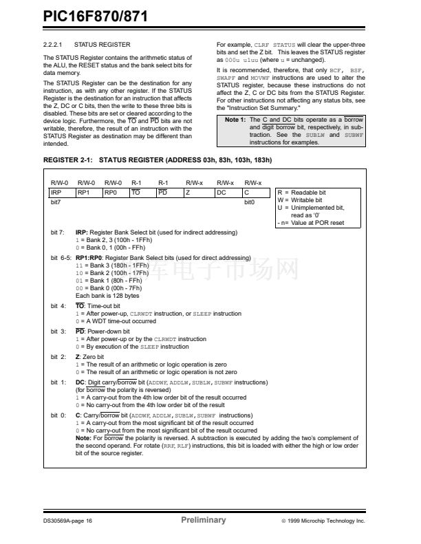
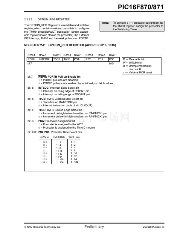
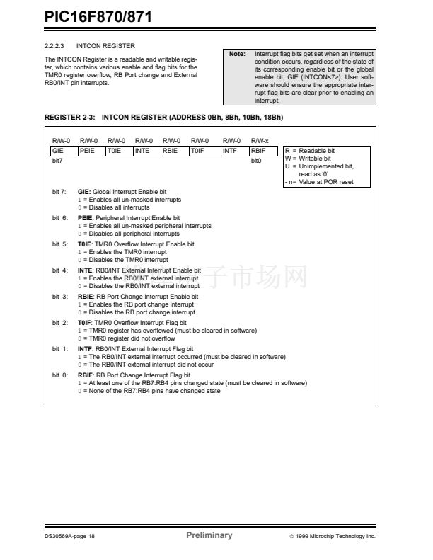
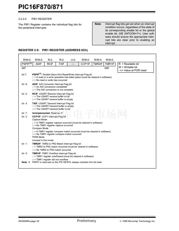
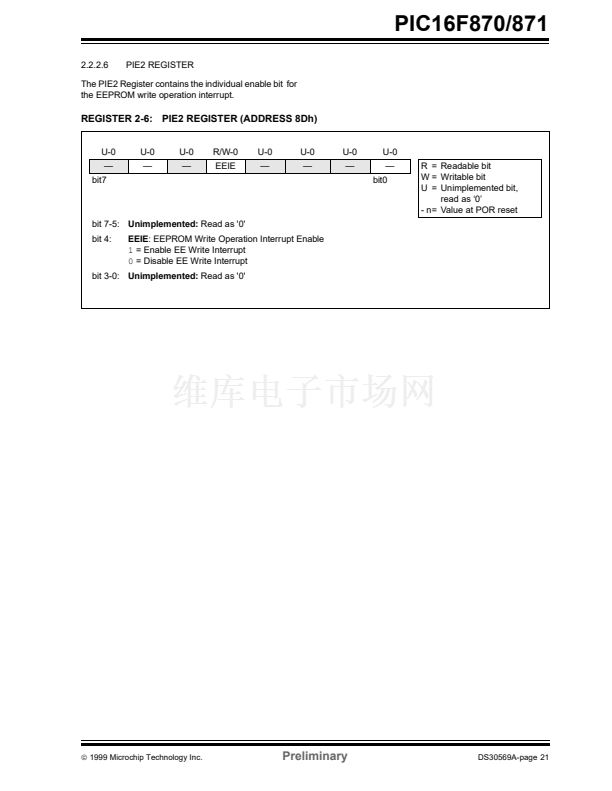
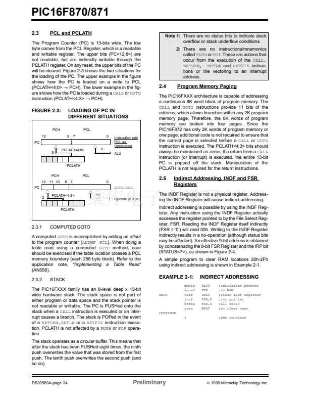
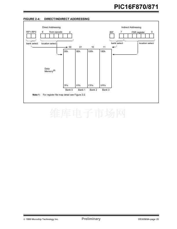
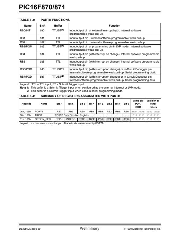
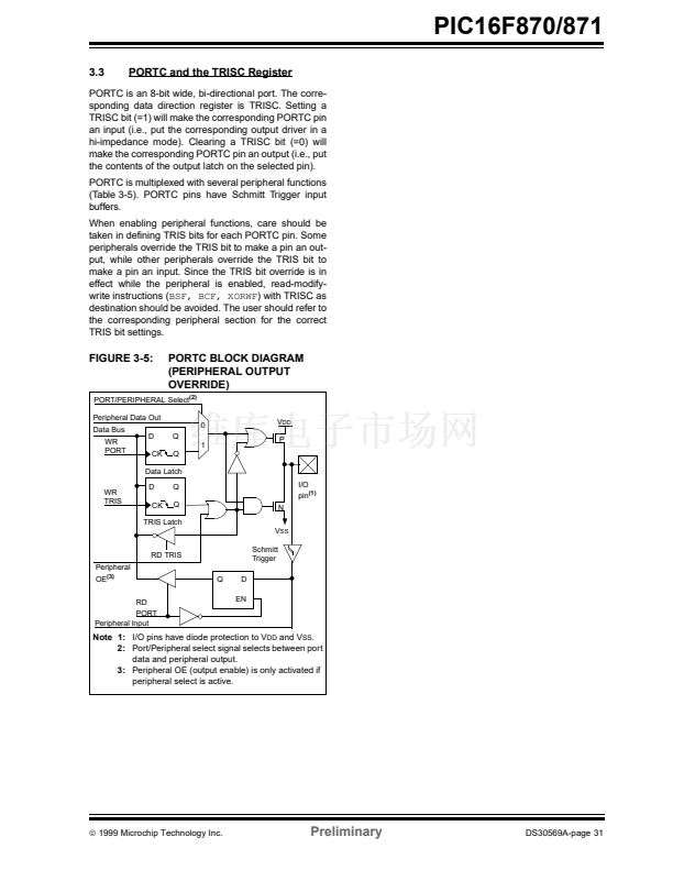
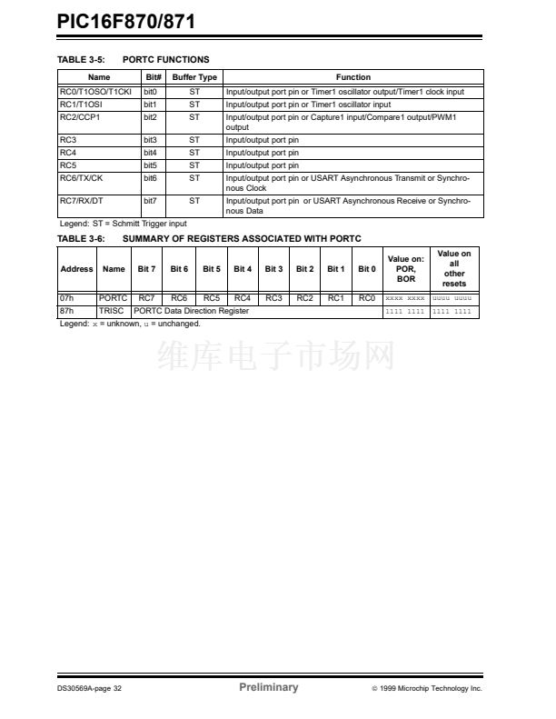
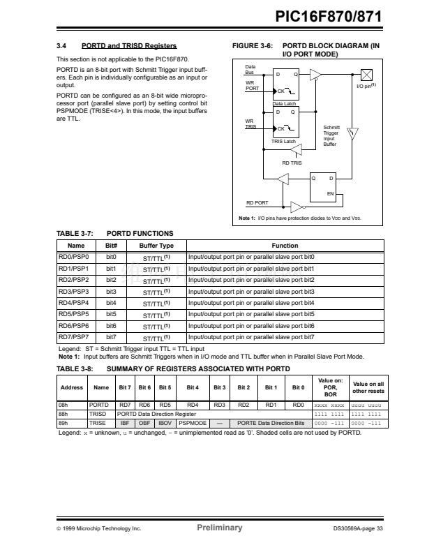
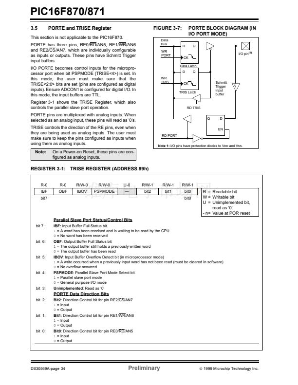
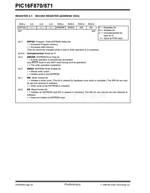
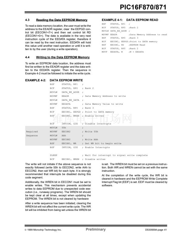
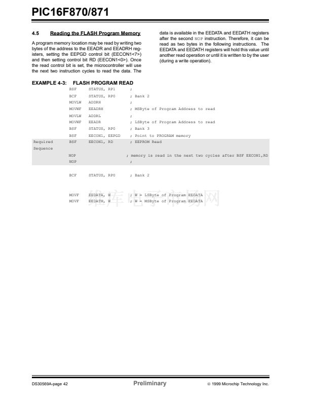
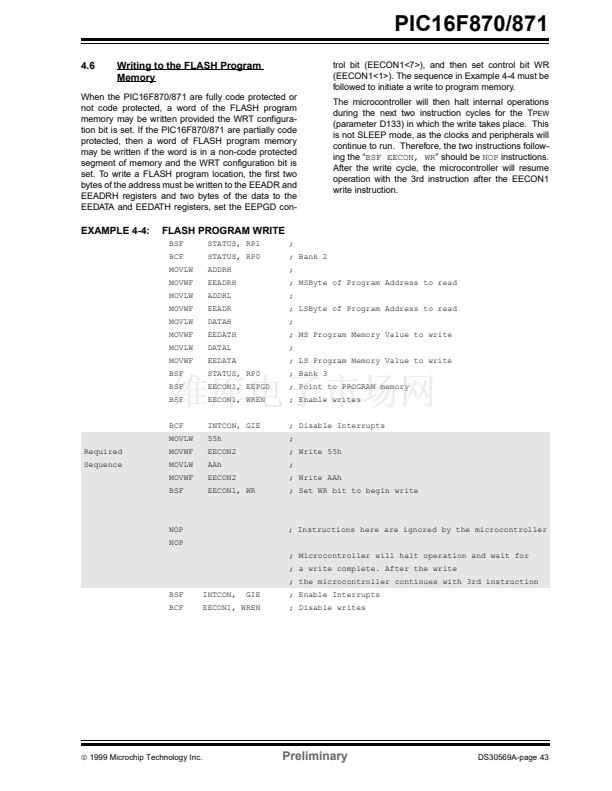
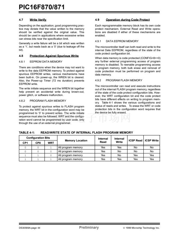
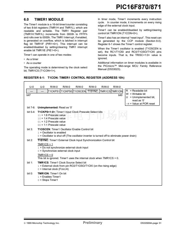
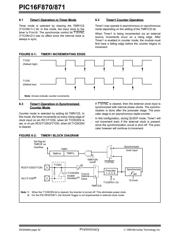
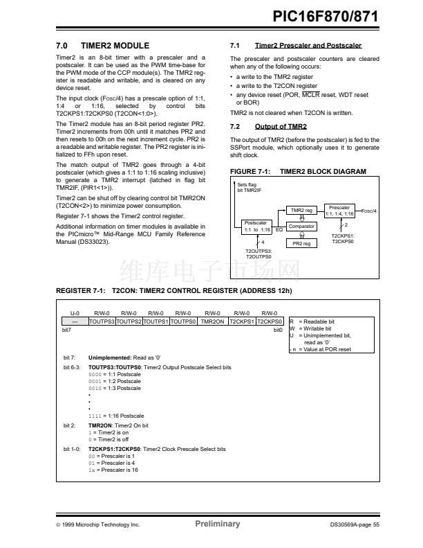
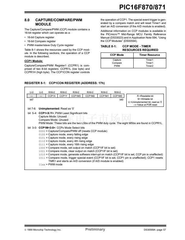
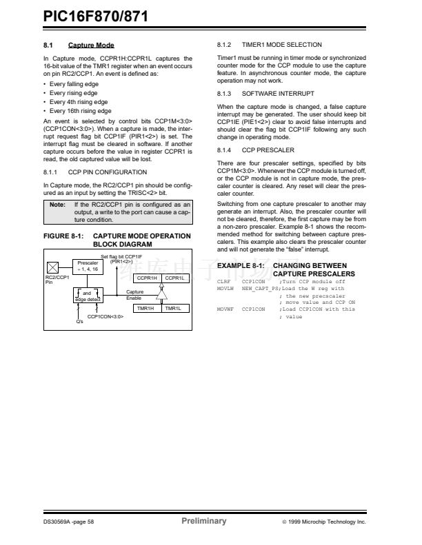
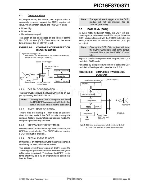
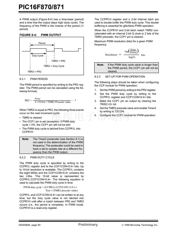
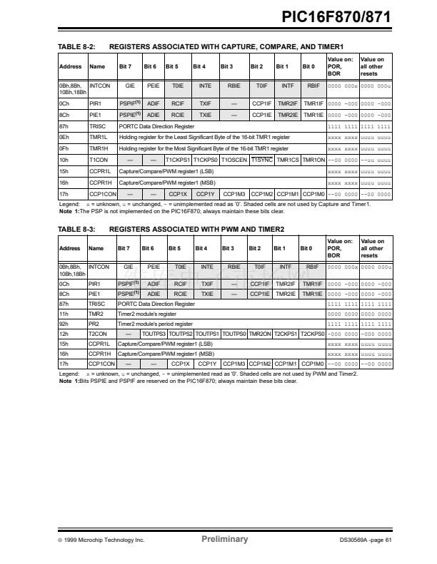
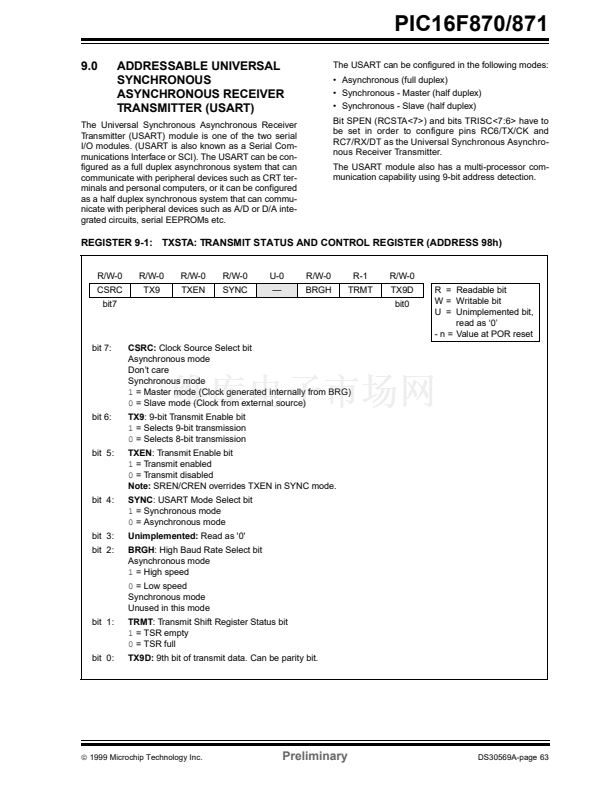
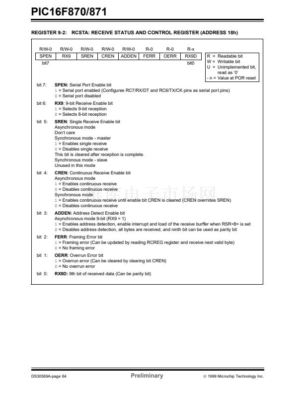
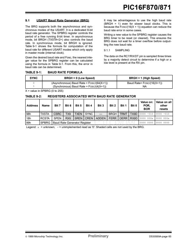
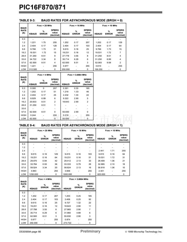
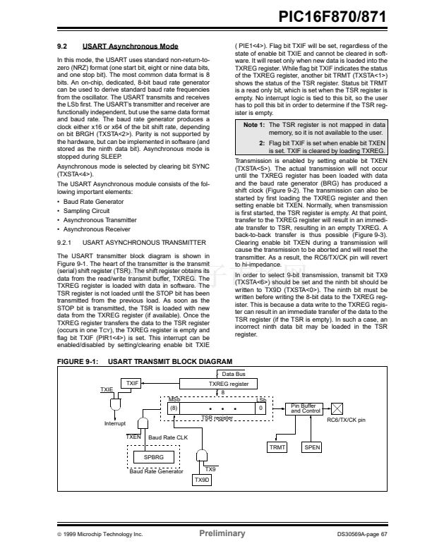
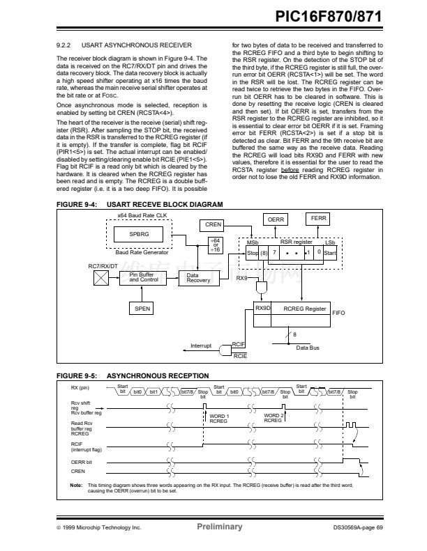
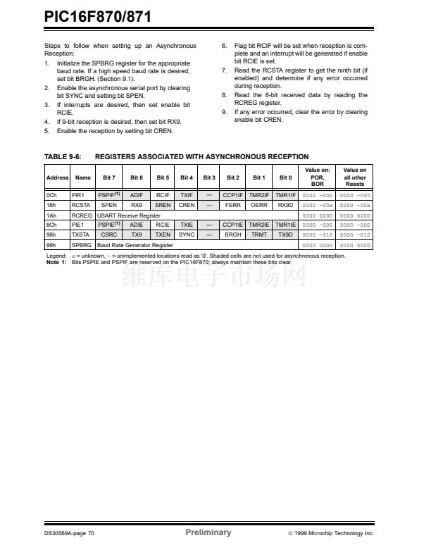
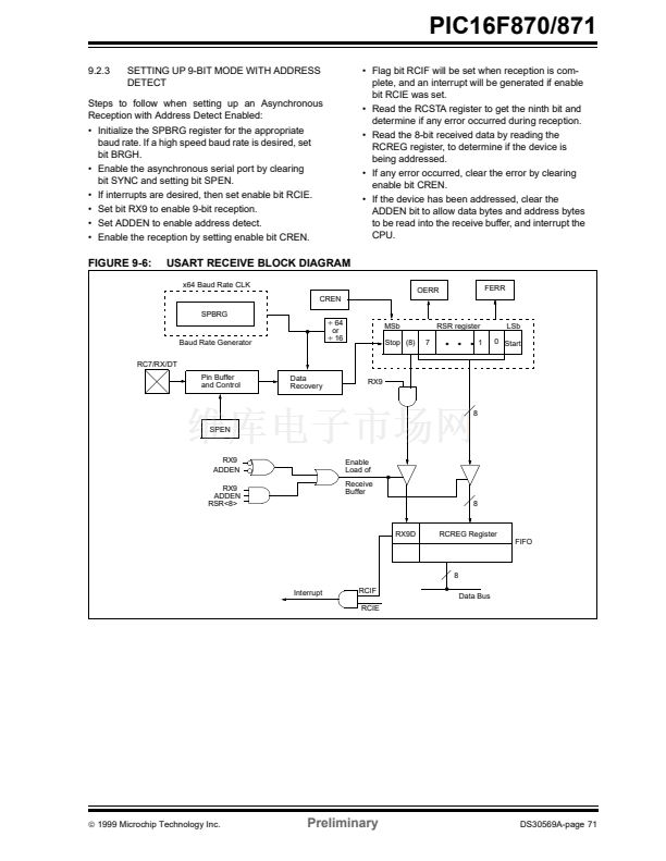
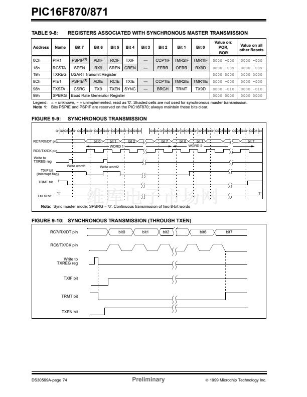
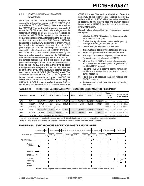
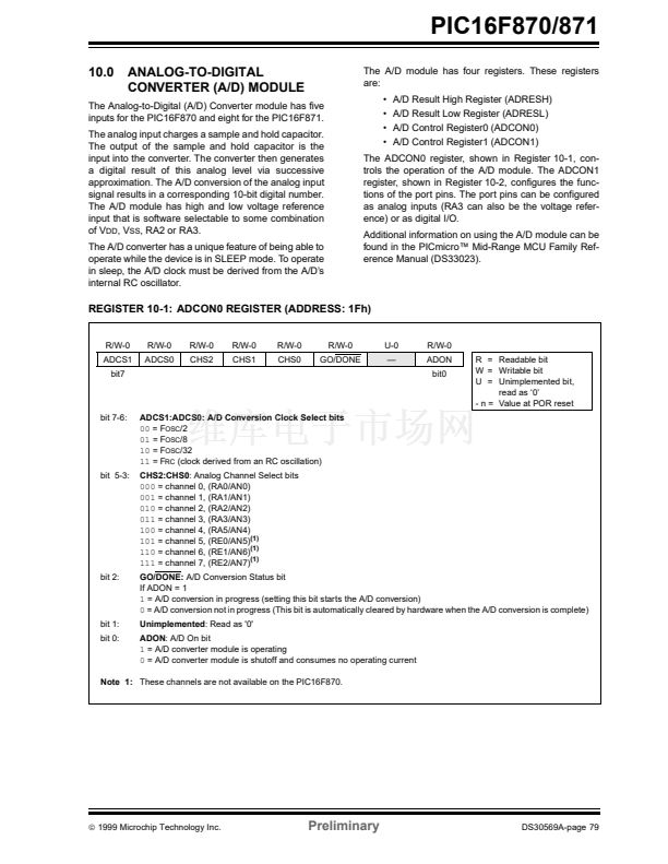
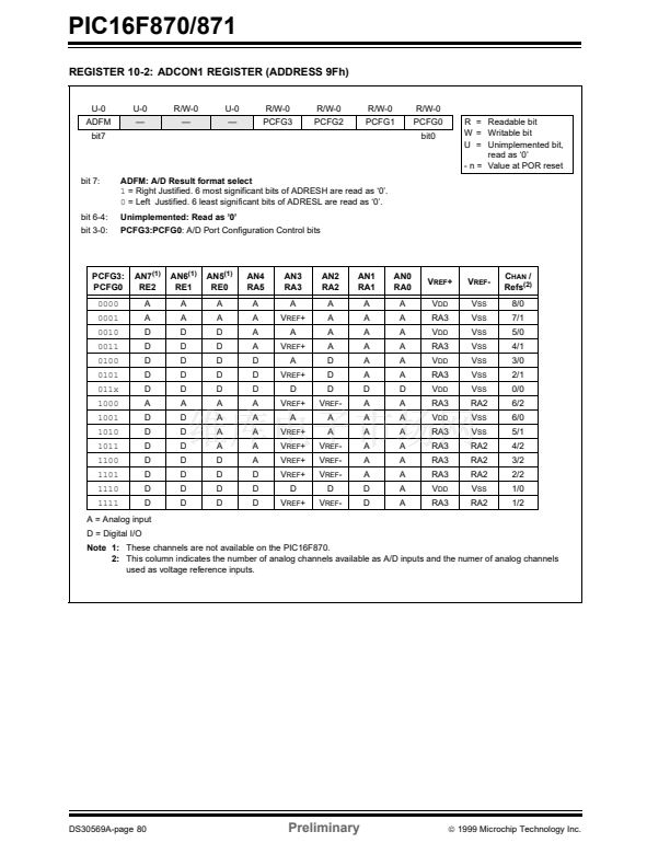
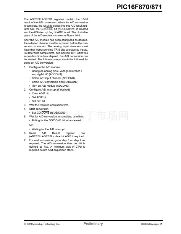
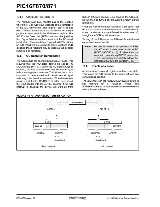
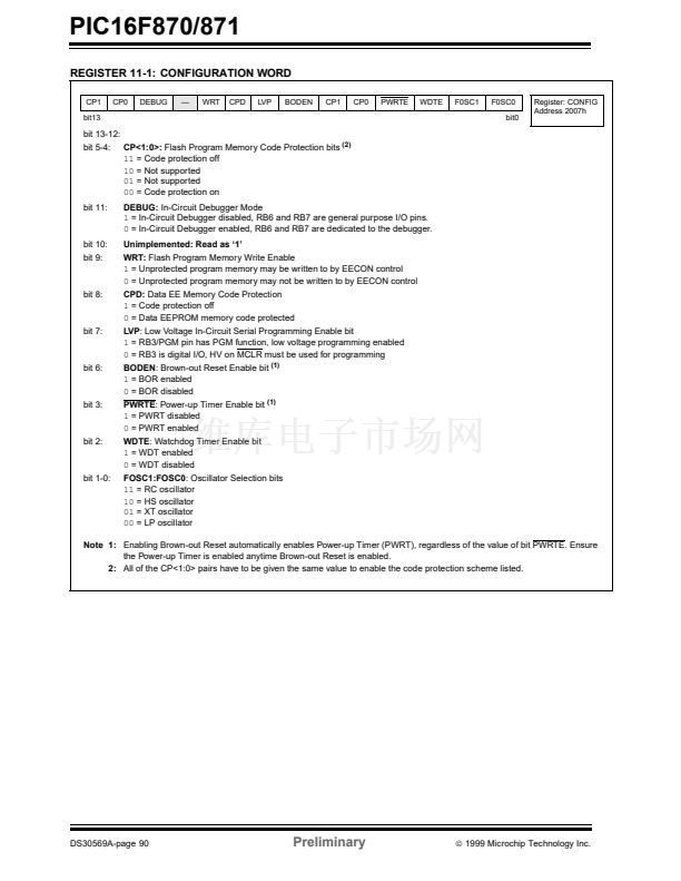
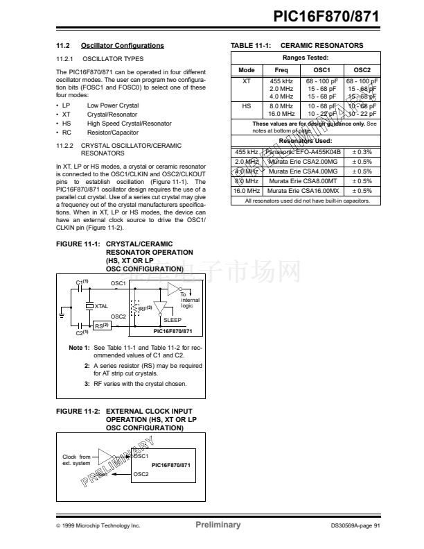
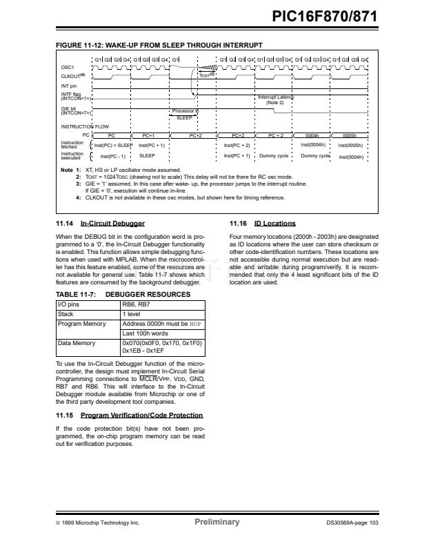
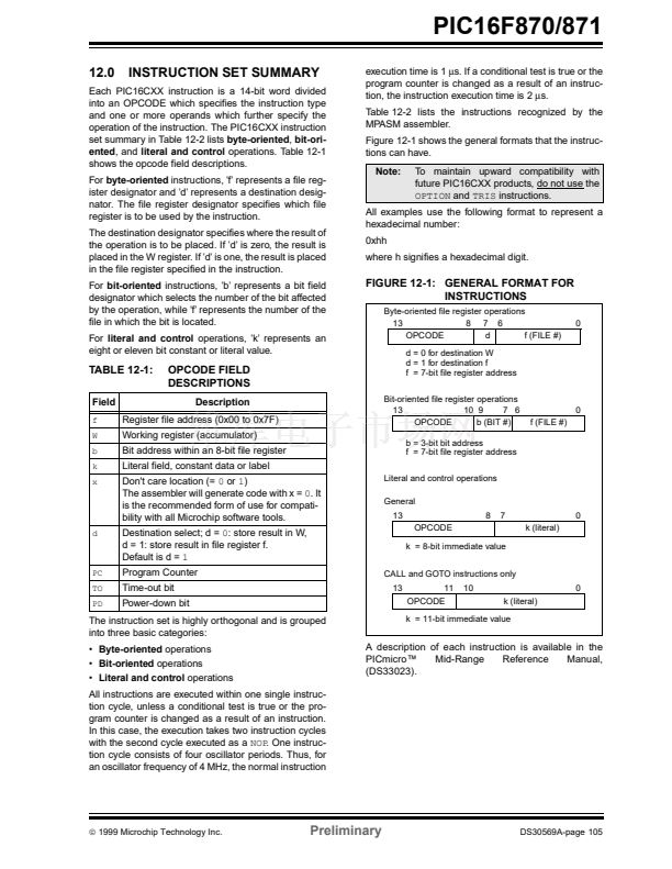
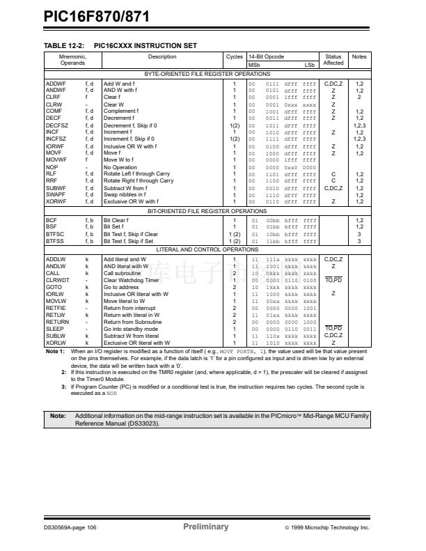
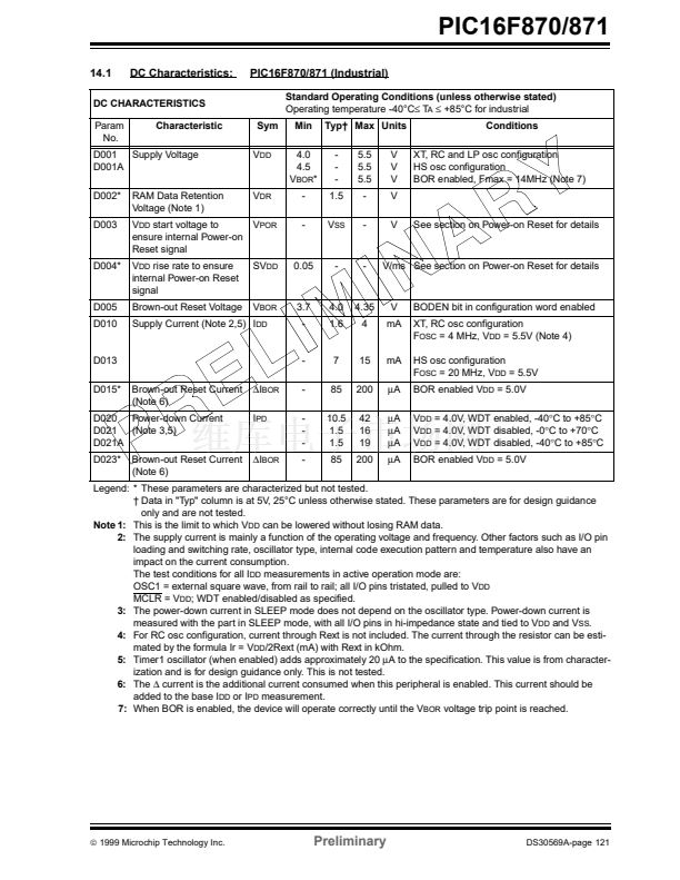
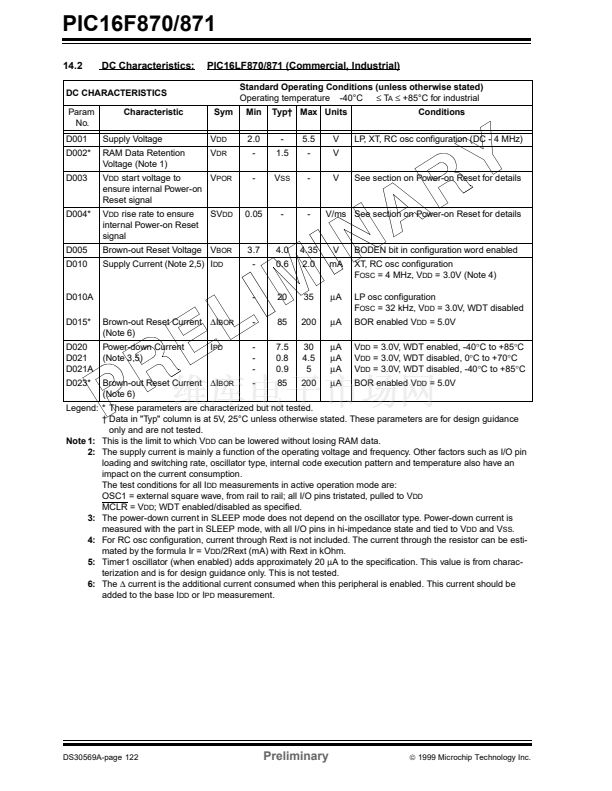
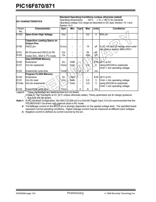
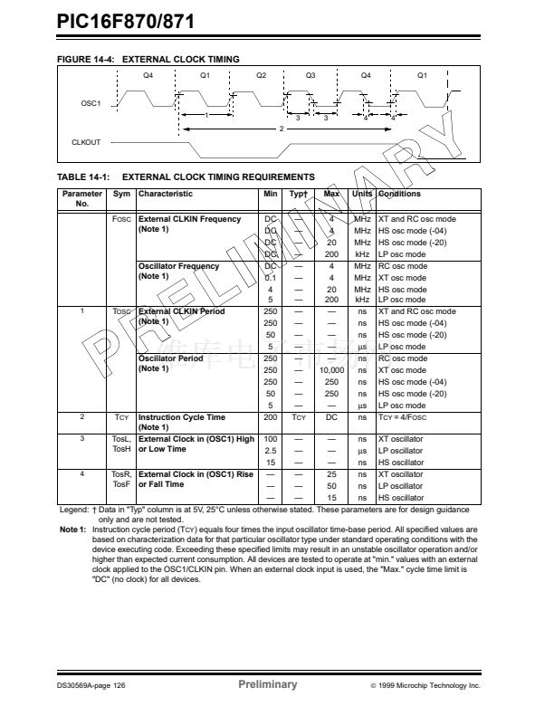
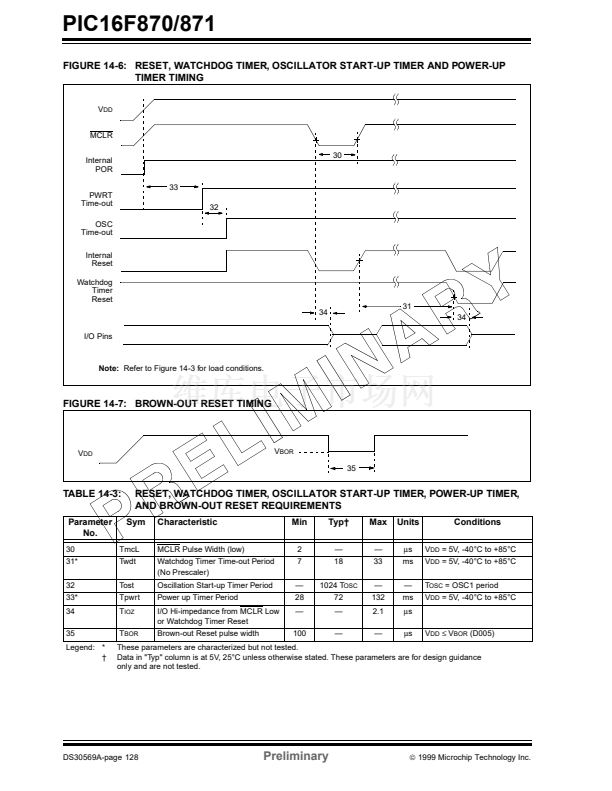
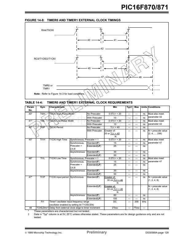
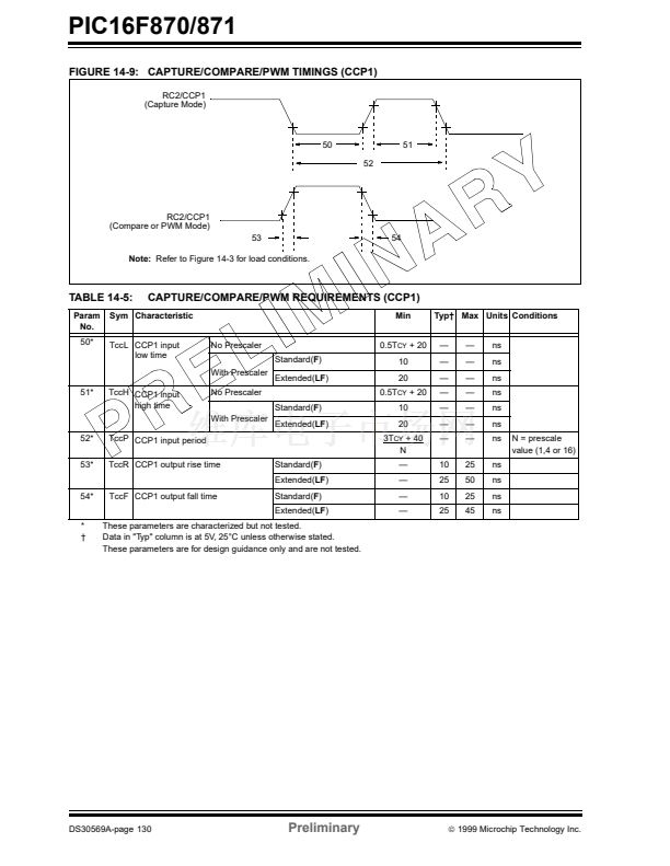
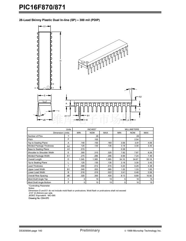
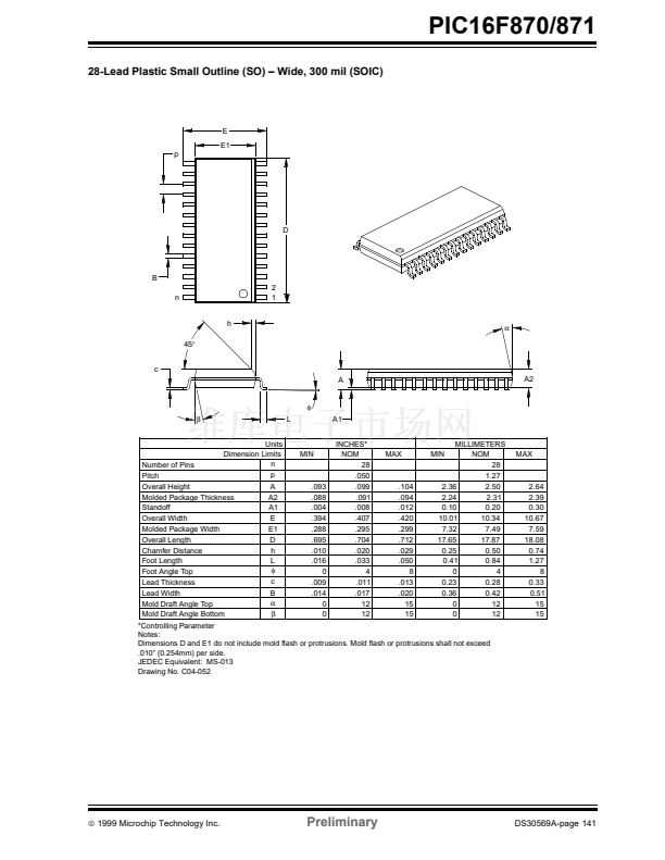
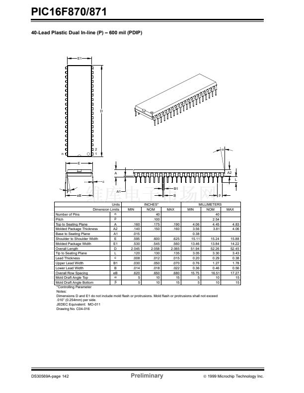
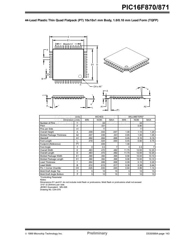
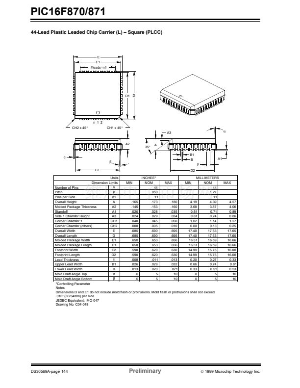
PIC16F870/871
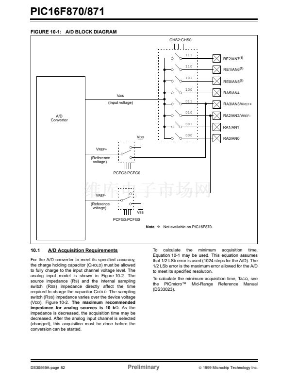
EQUATION 10-1:
T
ACQ
=
ACQUISITION TIME
Amplifier Settling Time +
Hold Capacitor Charging Time +
Temperature Coefficient
T
AMP
+ T
C
+ T
COFF
2碌S + T
C
+ [(Temperature -25掳C)(0.05碌S/掳C)]
C
HOLD
(R
IC
+ R
SS
+ R
S
) In(1/2047)
- 120pF (1k鈩?+ 7k鈩?+ 10k鈩? In(0.0004885)
16.47碌S
2碌S + 16.47碌S + [(50掳C -25脳C)(0.05碌S/脳C)
19.72碌S
T
C
T
ACQ
=
=
=
=
=
=
=
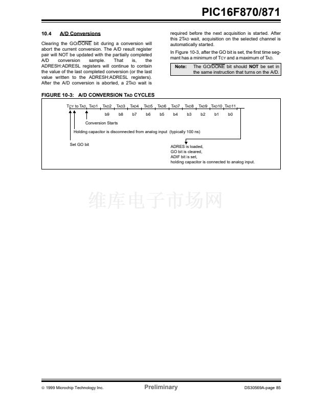
Note 1:
The reference voltage (V
REF
) has no effect on the equation, since it cancels itself out.
2:
The charge holding capacitor (C
HOLD
) is not discharged after each conversion.
3:
The maximum recommended impedance for analog sources is 10 k鈩? This is required to meet the pin leak-
age specification.
4:
After a conversion has completed, a 2.0T
AD
delay must complete before acquisition can begin again.
During this time, the holding capacitor is not connected to the selected A/D input channel.
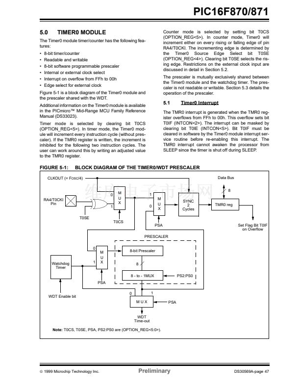
FIGURE 10-2: ANALOG INPUT MODEL
V
DD
R
S
VA
ANx
C
PIN
5 pF
V
T
= 0.6V
R
IC
鈮?/div>
1k
I
LEAKAGE
卤 500 nA
Sampling
Switch
SS R
SS
C
HOLD
= DAC capacitance
= 120 pF
V
SS
Legend C
PIN
= input capacitance
V
T
= threshold voltage
I
LEAKAGE
= leakage current at the pin due to
various junctions
R
IC
SS
C
HOLD
= interconnect resistance
= sampling switch
= sample/hold capacitance (from DAC)
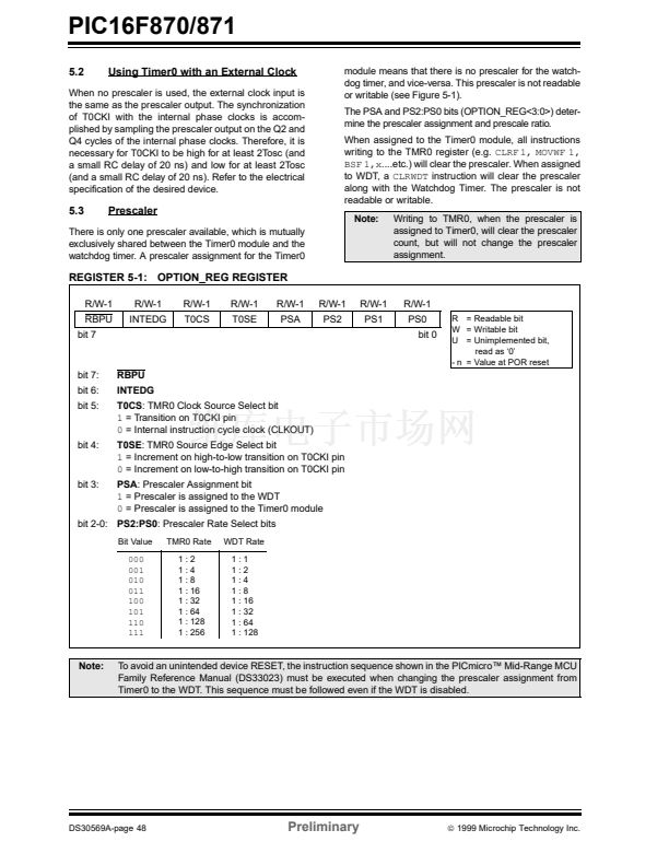
V
T
= 0.6V
6V
5V
V
DD
4V
3V
2V
5 6 7 8 9 10 11
Sampling Switch
( k鈩?)
漏
1999 Microchip Technology Inc.
Preliminary
DS30569A-page 83


 1
1
 2
2
 3
3
 4
4
 5
5
 6
6
 7
7
 8
8
 9
9
 10
10
 11
11
 12
12
 13
13
 14
14
 15
15
 16
16
 17
17
 18
18
 19
19
 20
20
 21
21
 22
22
 23
23
 24
24
 25
25
 26
26
 27
27
 28
28
 29
29
 30
30
 31
31
 32
32
 33
33
 34
34
 35
35
 36
36
 37
37
 38
38
 39
39
 40
40
 41
41
 42
42
 43
43
 44
44
 45
45
 46
46
 47
47
 48
48
 49
49
 50
50
 51
51
 52
52
 53
53
 54
54
 55
55
 56
56
 57
57
 58
58
 59
59
 60
60
 61
61
 62
62
 63
63
 64
64
 65
65
 66
66
 67
67
 68
68
 69
69
 70
70
 71
71
 72
72
 73
73
 74
74
 75
75
 76
76
 77
77
 78
78
 79
79
 80
80
 81
81
 82
82
 83
83
 84
84
 85
85
 86
86
 87
87
 88
88
 89
89
 90
90
 91
91
 92
92
 93
93
 94
94
 95
95
 96
96
 97
97
 98
98
 99
99
 100
100
 101
101
 102
102
 103
103
 104
104
 105
105
 106
106
 107
107
 108
108
 109
109
 110
110
 111
111
 112
112
 113
113
 114
114
 115
115
 116
116
 117
117
 118
118
 119
119
 120
120
 121
121
 122
122
 123
123
 124
124
 125
125
 126
126
 127
127
 128
128
 129
129
 130
130
 131
131
 132
132
 133
133
 134
134
 135
135
 136
136
 137
137
 138
138
 139
139
 140
140
 141
141
 142
142
 143
143
 144
144
 145
145
 146
146
 147
147
 148
148
 149
149
 150
150
 151
151
 152
152
 153
153
 154
154
 155
155
 156
156
