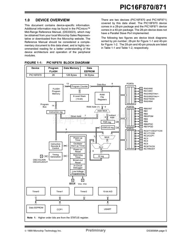
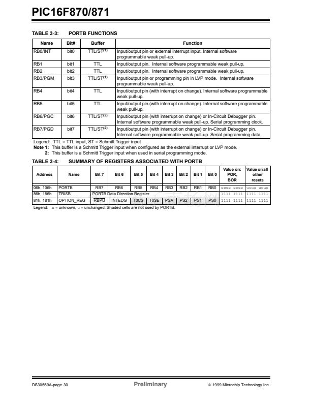
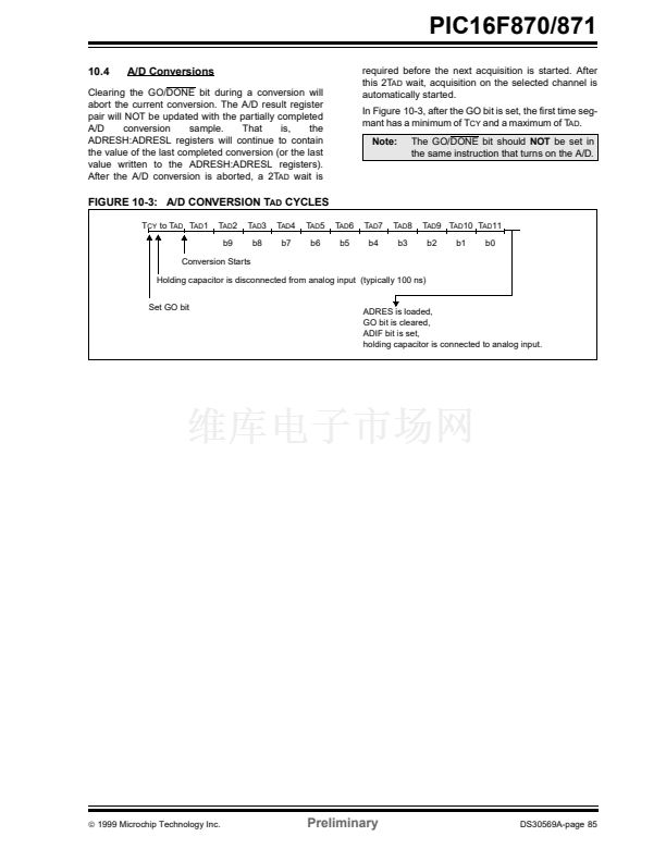
= In-Circuit Debugger disabled, RB6 and RB7 are general purpose I/O pins.
= In-Circuit Debugger enabled, RB6 and RB7 are dedicated to the debugger.
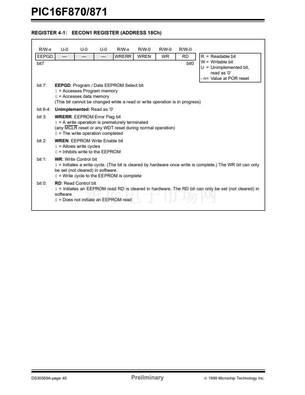
Unimplemented: Read as 鈥?鈥?/div>
WRT:
Flash Program Memory Write Enable
1
= Unprotected program memory may be written to by EECON control
0
= Unprotected program memory may not be written to by EECON control
CPD:
Data EE Memory Code Protection
1
= Code protection off
0
= Data EEPROM memory code protected
LVP:
Low Voltage In-Circuit Serial Programming Enable bit
1
= RB3/PGM pin has PGM function, low voltage programming enabled
0
= RB3 is digital I/O, HV on MCLR must be used for programming
BODEN:
Brown-out Reset Enable bit
(1)
1
= BOR enabled
0
= BOR disabled
PWRTE:
Power-up Timer Enable bit
(1)
1
= PWRT disabled
0
= PWRT enabled
WDTE:
Watchdog Timer Enable bit
1
= WDT enabled
0
= WDT disabled
FOSC1:FOSC0:
Oscillator Selection bits
11
= RC oscillator
10
= HS oscillator
01
= XT oscillator
00
= LP oscillator
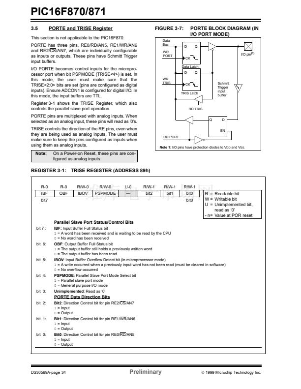
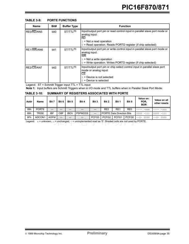
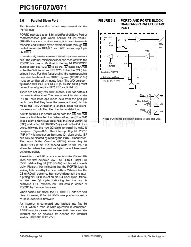
bit 11:
bit 10:
bit 9:
bit 8:
bit 7:
bit 6:
bit 3:
bit 2:
bit 1-0:
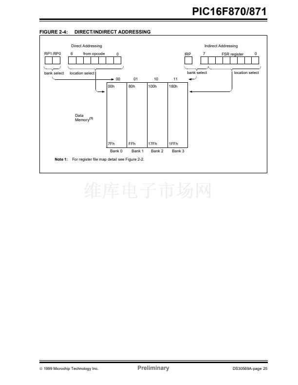
Note 1:
Enabling Brown-out Reset automatically enables Power-up Timer (PWRT), regardless of the value of bit PWRTE. Ensure
the Power-up Timer is enabled anytime Brown-out Reset is enabled.
2:
All of the CP<1:0> pairs have to be given the same value to enable the code protection scheme listed.
DS30569A-page 90
Preliminary
漏
1999 Microchip Technology Inc.


 1
1
 2
2
 3
3
 4
4
 5
5
 6
6
 7
7
 8
8
 9
9
 10
10
 11
11
 12
12
 13
13
 14
14
 15
15
 16
16
 17
17
 18
18
 19
19
 20
20
 21
21
 22
22
 23
23
 24
24
 25
25
 26
26
 27
27
 28
28
 29
29
 30
30
 31
31
 32
32
 33
33
 34
34
 35
35
 36
36
 37
37
 38
38
 39
39
 40
40
 41
41
 42
42
 43
43
 44
44
 45
45
 46
46
 47
47
 48
48
 49
49
 50
50
 51
51
 52
52
 53
53
 54
54
 55
55
 56
56
 57
57
 58
58
 59
59
 60
60
 61
61
 62
62
 63
63
 64
64
 65
65
 66
66
 67
67
 68
68
 69
69
 70
70
 71
71
 72
72
 73
73
 74
74
 75
75
 76
76
 77
77
 78
78
 79
79
 80
80
 81
81
 82
82
 83
83
 84
84
 85
85
 86
86
 87
87
 88
88
 89
89
 90
90
 91
91
 92
92
 93
93
 94
94
 95
95
 96
96
 97
97
 98
98
 99
99
 100
100
 101
101
 102
102
 103
103
 104
104
 105
105
 106
106
 107
107
 108
108
 109
109
 110
110
 111
111
 112
112
 113
113
 114
114
 115
115
 116
116
 117
117
 118
118
 119
119
 120
120
 121
121
 122
122
 123
123
 124
124
 125
125
 126
126
 127
127
 128
128
 129
129
 130
130
 131
131
 132
132
 133
133
 134
134
 135
135
 136
136
 137
137
 138
138
 139
139
 140
140
 141
141
 142
142
 143
143
 144
144
 145
145
 146
146
 147
147
 148
148
 149
149
 150
150
 151
151
 152
152
 153
153
 154
154
 155
155
 156
156
