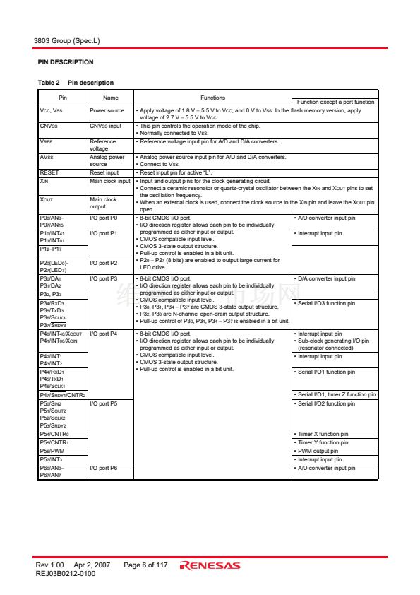
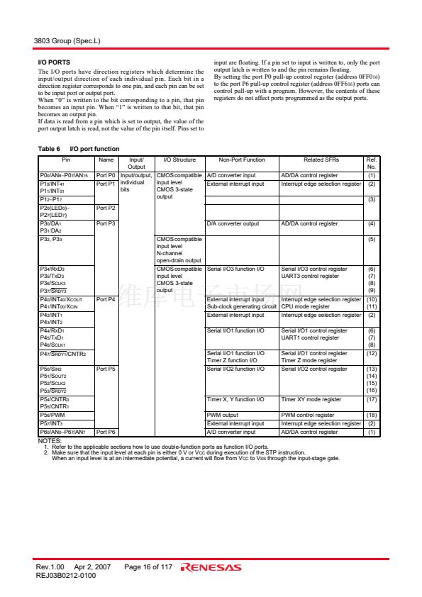
7. Transmit interrupt request when transmit enable bit is set
sequence.
1. Set the serial I/O3 transmit interrupt enable bit to 鈥?鈥?(dis-
abled).
2. Set the transmit enable bit to 鈥?鈥?
3. Set the serial I/O3 transmit interrupt request bit to 鈥?鈥?after
1 or more instruction has executed.
4. Set the serial I/O3 transmit interrupt enable bit to 鈥?鈥?/div>
(enabled).
鈥?Reason
When the transmit enable bit is set to 鈥?鈥? the transmit buffer
empty flag and the transmit shift register shift completion flag
are also set to 鈥?鈥? Therefore, regardless of selecting which
timing for the generating of transmit interrupts, the interrupt
request is generated and the transmit interrupt request bit is set
at this point.
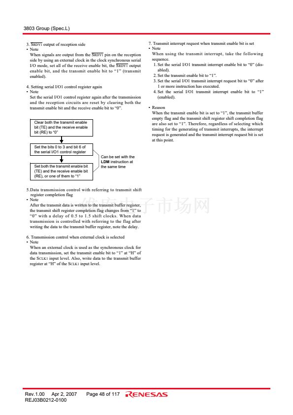
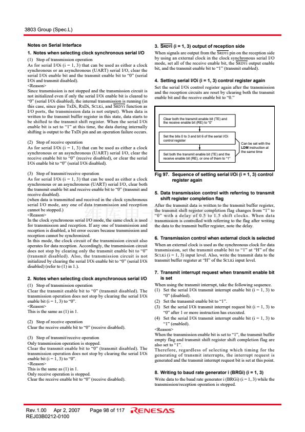
Set the bits 0 to 3 and bit 6 of
the serial I/O3 control register
Can be set with the
LDM
instruction at
the same time
Set both the transmit enable bit
(TE) and the receive enable bit
(RE), or one of them to 鈥?鈥?/div>
5.Data transmission control with referring to transmit shift
register completion flag
鈥?Note
After the transmit data is written to the transmit buffer register,
the transmit shift register completion flag changes from 鈥?鈥?to
鈥?鈥?with a delay of 0.5 to 1.5 shift clocks. When data
transmission is controlled with referring to the flag after
writing the data to the transmit buffer register, note the delay.
6. Transmission control when external clock is selected
鈥?Note
When an external clock is used as the synchronous clock for
data transmission, set the transmit enable bit to 鈥?鈥?at 鈥淗鈥?of
the S
CLK3
input level. Also, write data to the transmit buffer
register at 鈥淗鈥?of the S
CLK
input level.
Rev.1.00 Apr 2, 2007
REJ03B0212-0100
Page 56 of 117


 1
1
 2
2
 3
3
 4
4
 5
5
 6
6
 7
7
 8
8
 9
9
 10
10
 11
11
 12
12
 13
13
 14
14
 15
15
 16
16
 17
17
 18
18
 19
19
 20
20
 21
21
 22
22
 23
23
 24
24
 25
25
 26
26
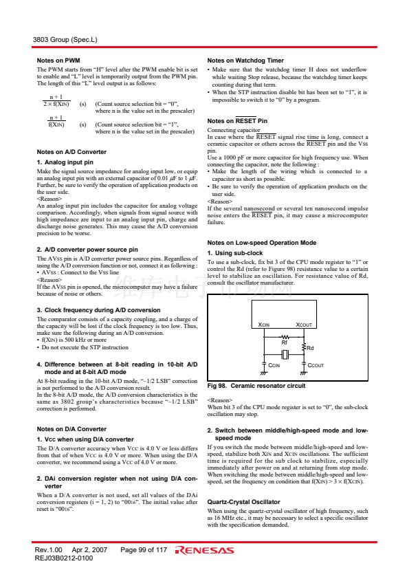
 27
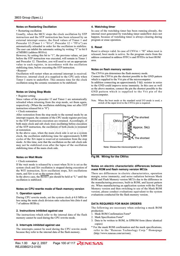
27
 28
28
 29
29
 30
30
 31
31
 32
32
 33
33
 34
34
 35
35
 36
36
 37
37
 38
38
 39
39
 40
40
 41
41
 42
42
 43
43
 44
44
 45
45
 46
46
 47
47
 48
48
 49
49
 50
50
 51
51
 52
52
 53
53
 54
54
 55
55
 56
56
 57
57
 58
58
 59
59
 60
60
 61
61
 62
62
 63
63
 64
64
 65
65
 66
66
 67
67
 68
68
 69
69
 70
70
 71
71
 72
72
 73
73
 74
74
 75
75
 76
76
 77
77
 78
78
 79
79
 80
80
 81
81
 82
82
 83
83
 84
84
 85
85
 86
86
 87
87
 88
88
 89
89
 90
90
 91
91
 92
92
 93
93
 94
94
 95
95
 96
96
 97
97
 98
98
 99
99
 100
100
 101
101
 102
102
 103
103
 104
104
 105
105
 106
106
 107
107
 108
108
 109
109
 110
110
 111
111
 112
112
 113
113
 114
114
 115
115
 116
116
 117
117
 118
118
 119
119
