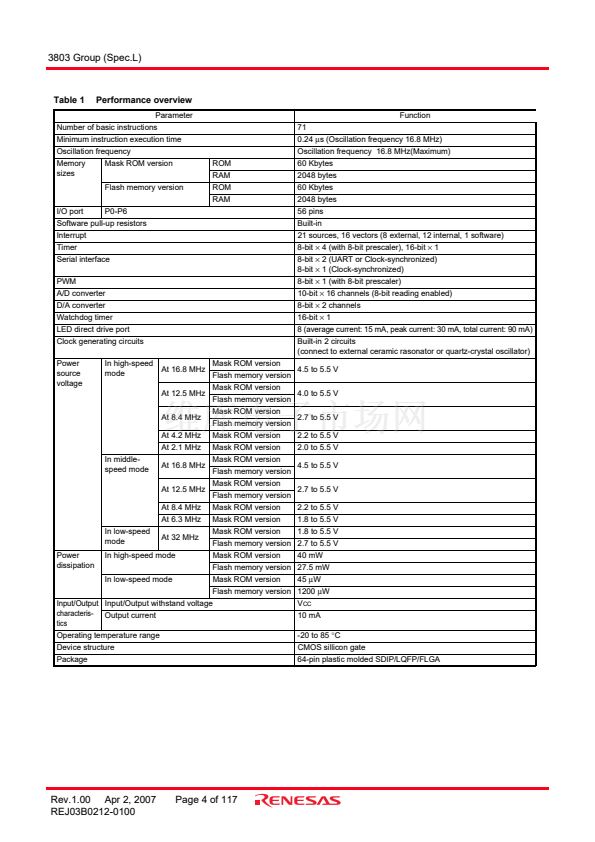
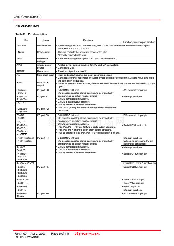
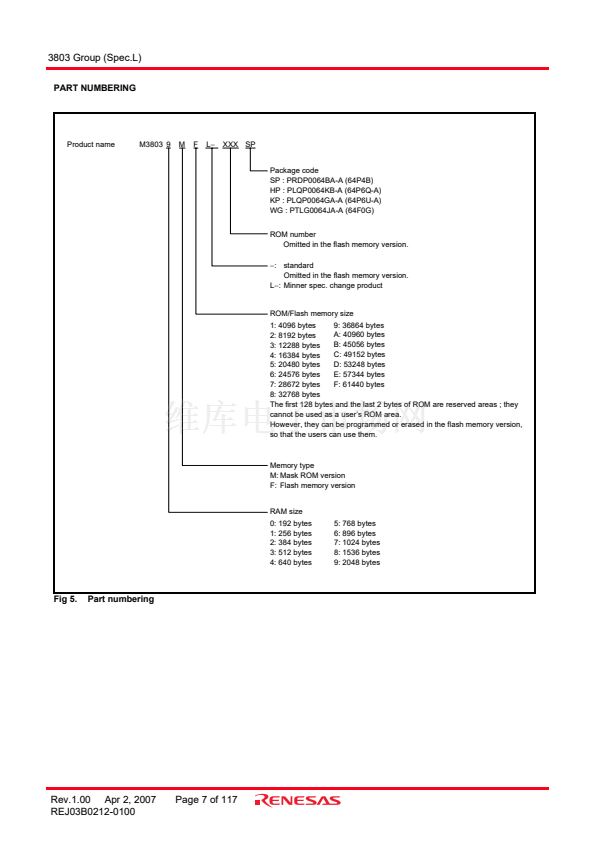
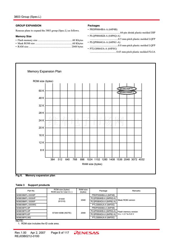
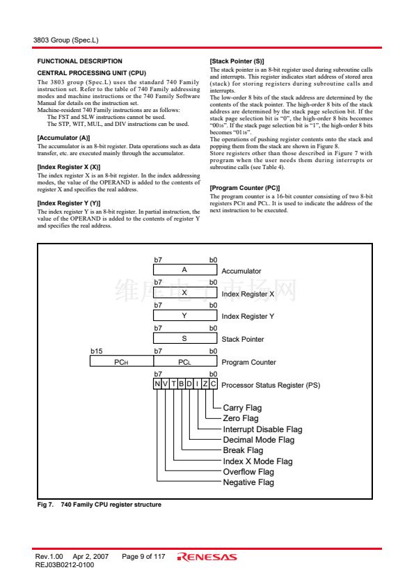
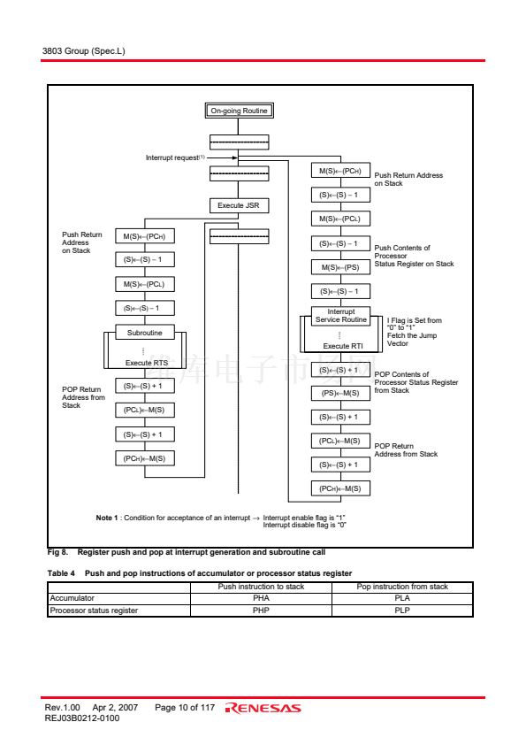
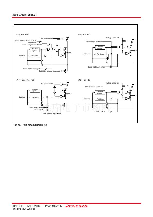
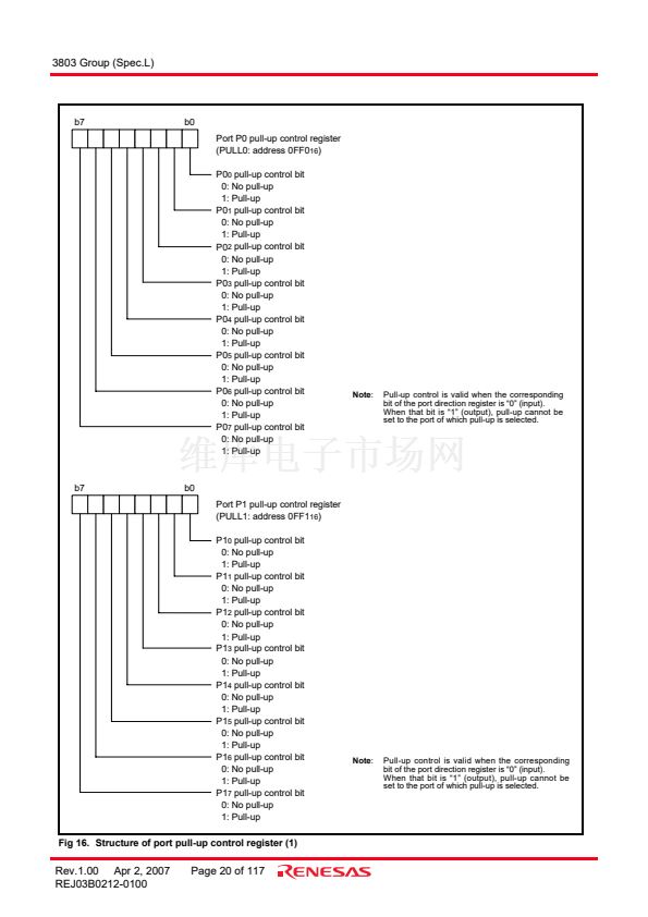
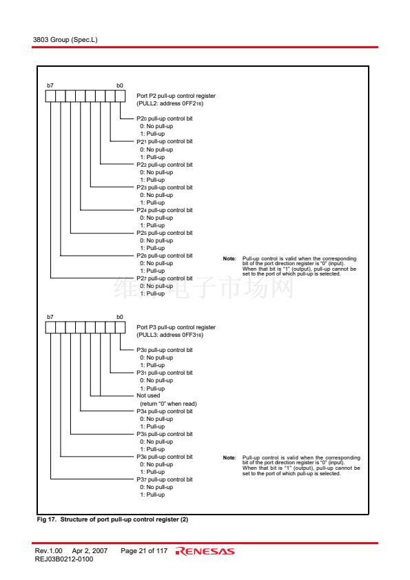
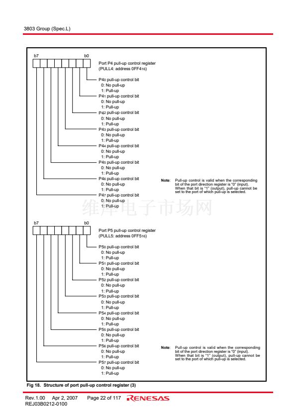
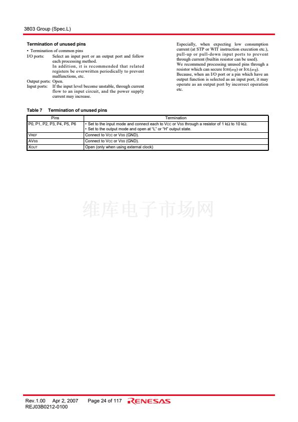
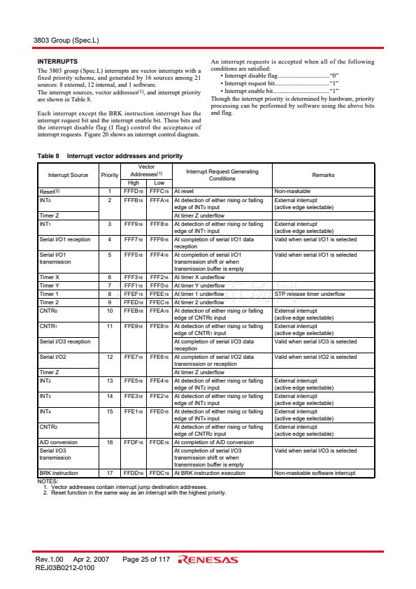
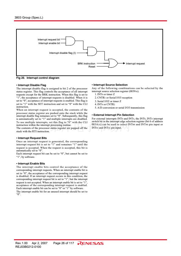
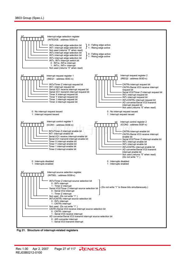
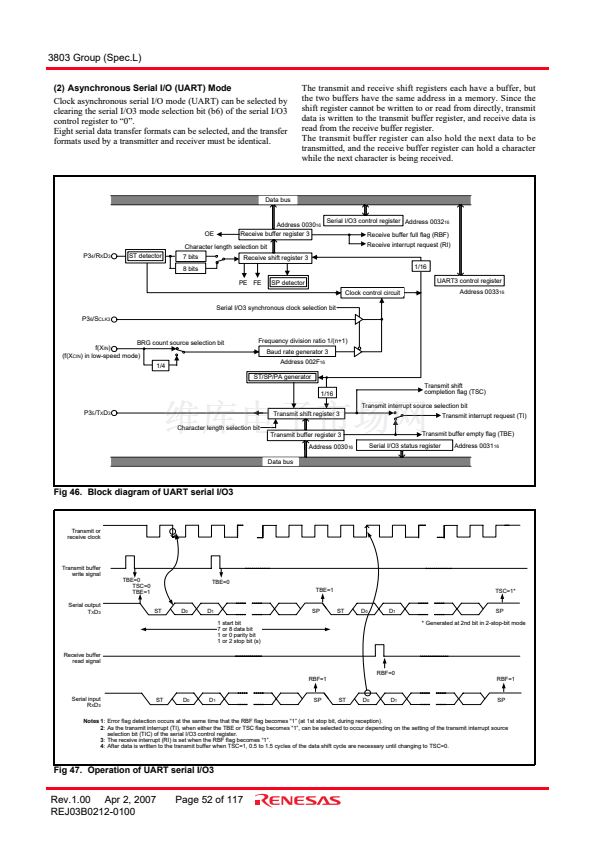
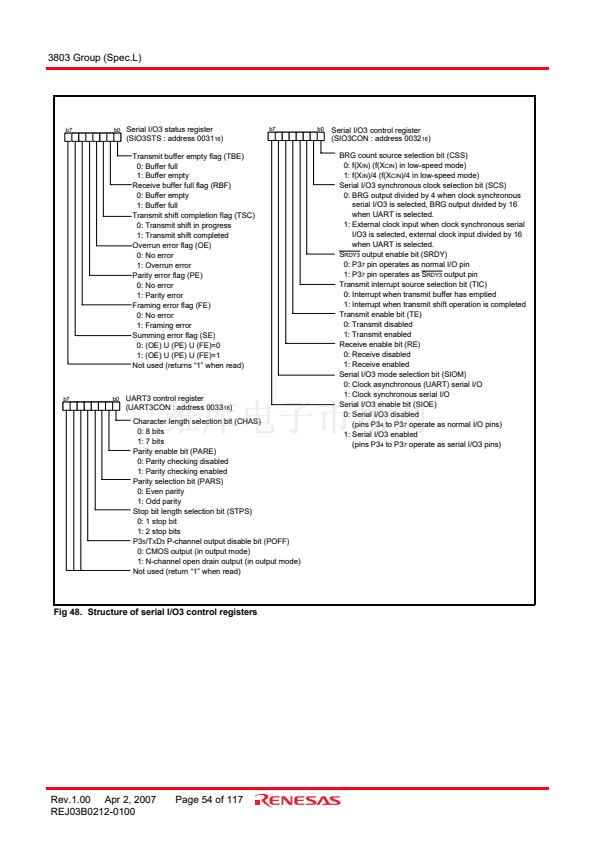
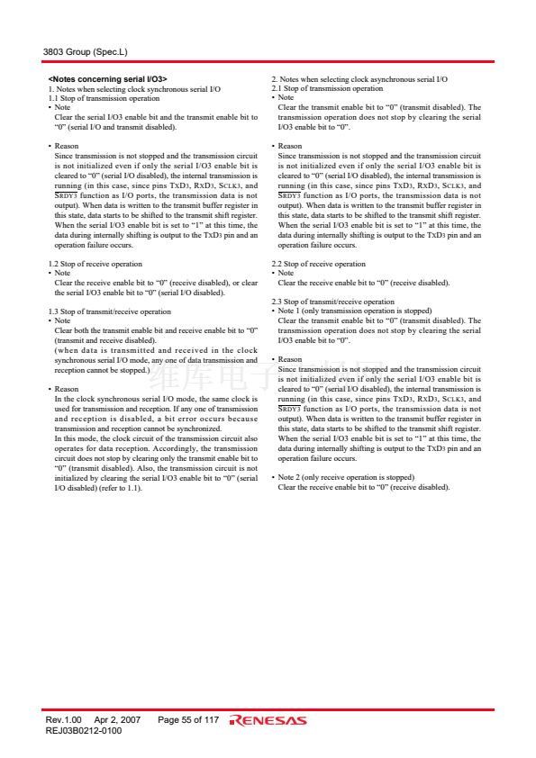
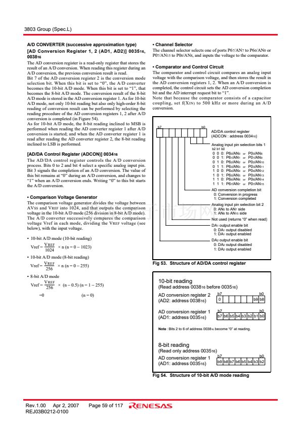
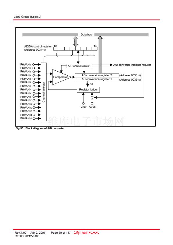
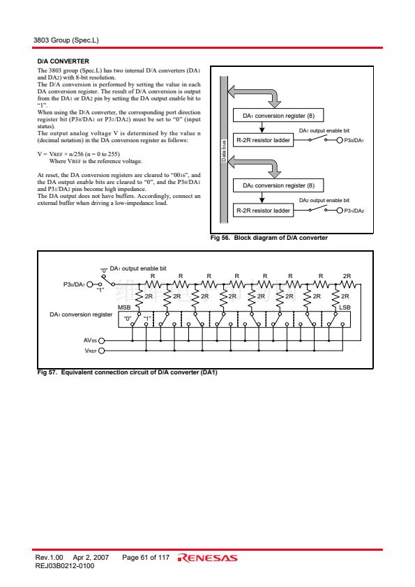
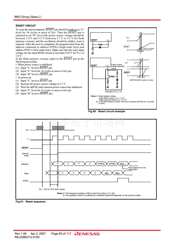
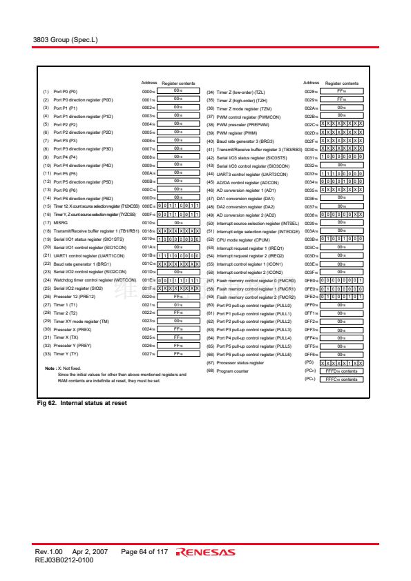
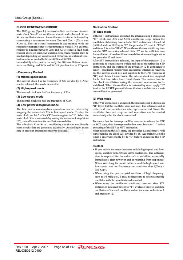
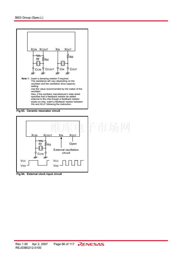
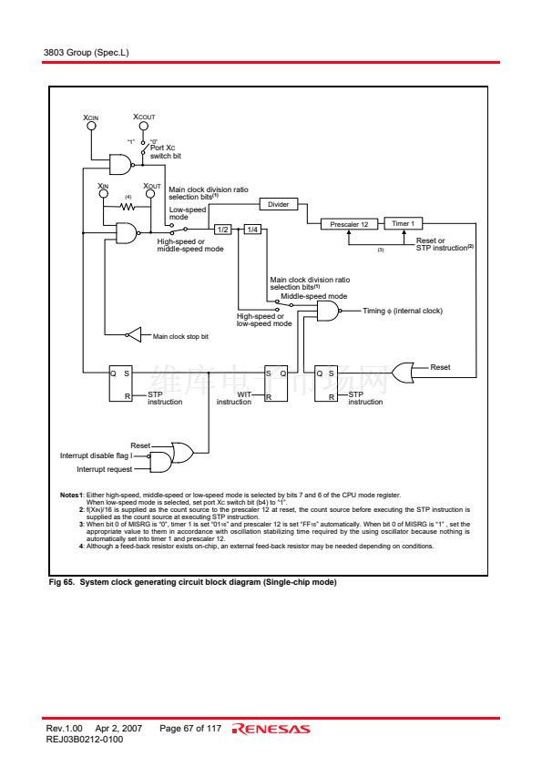
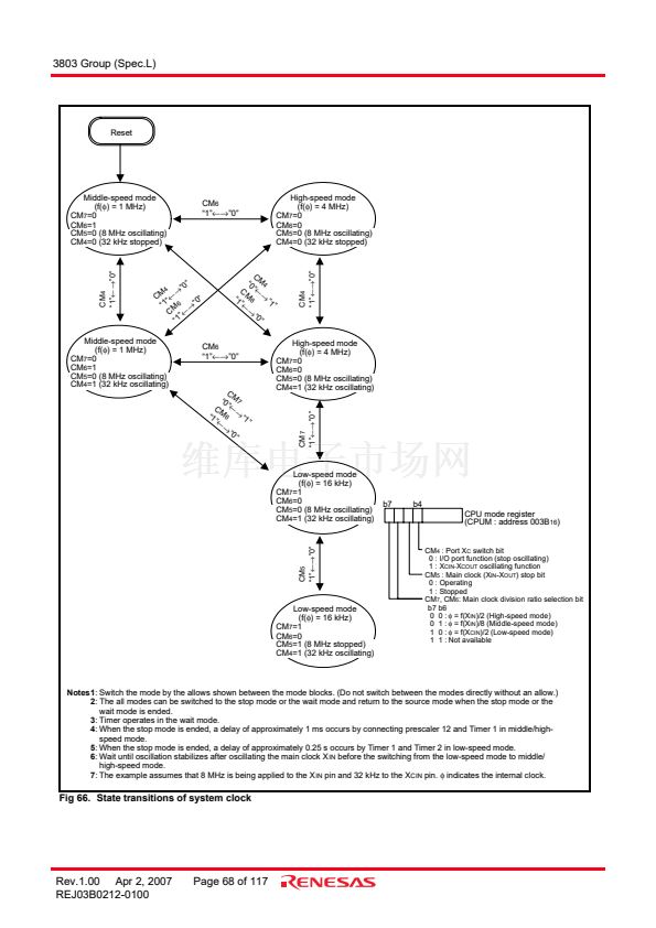
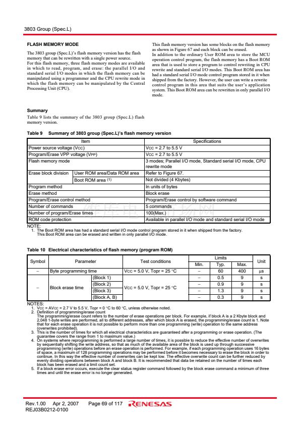
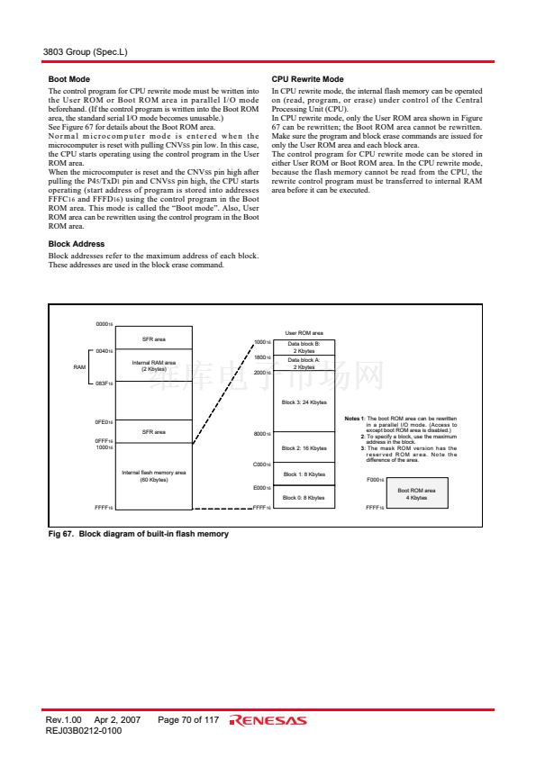
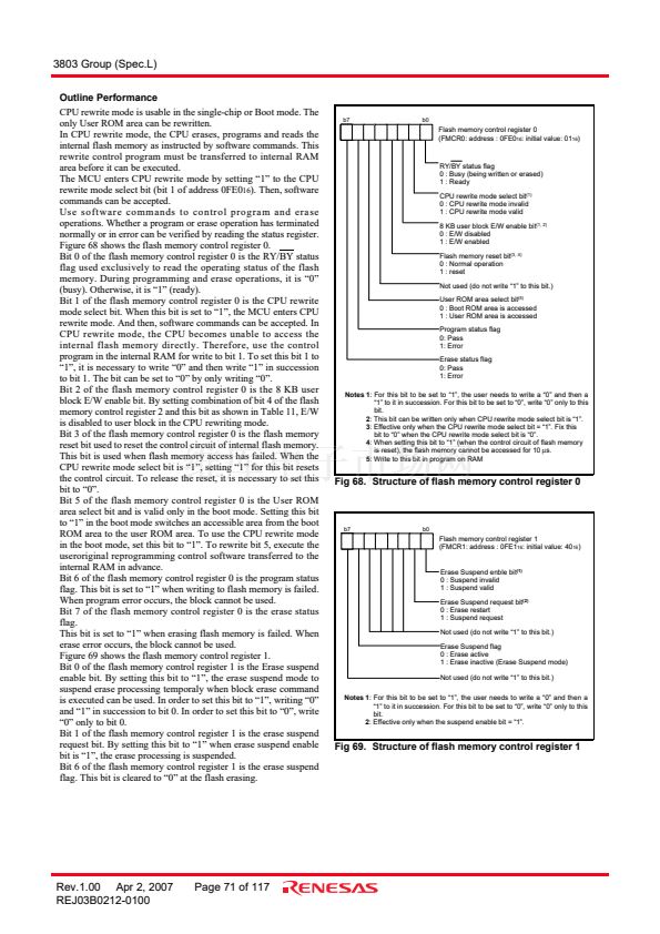
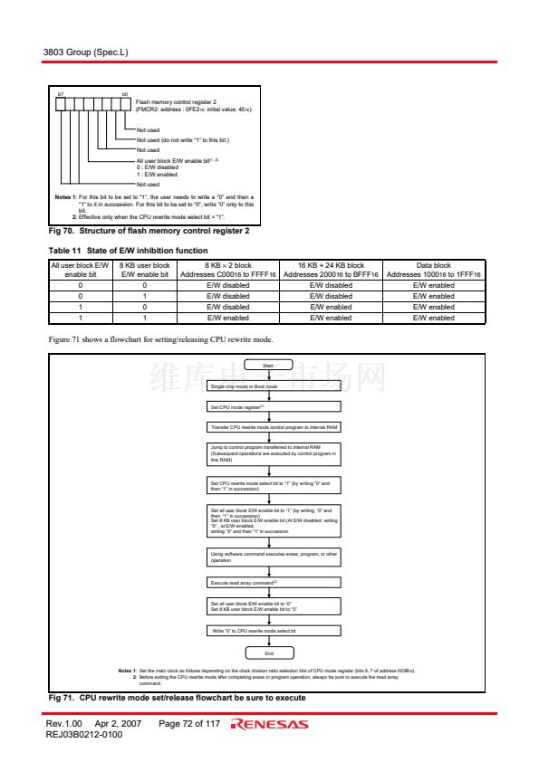
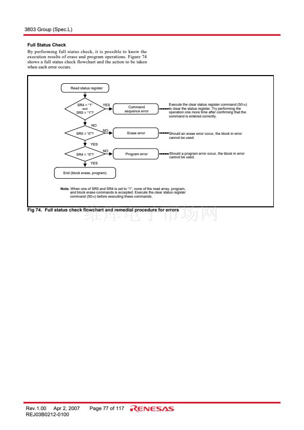
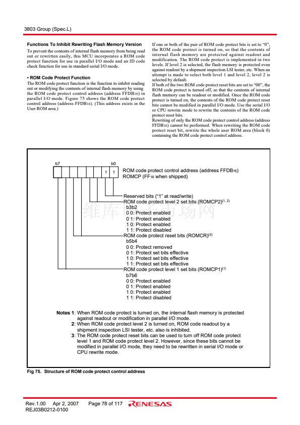
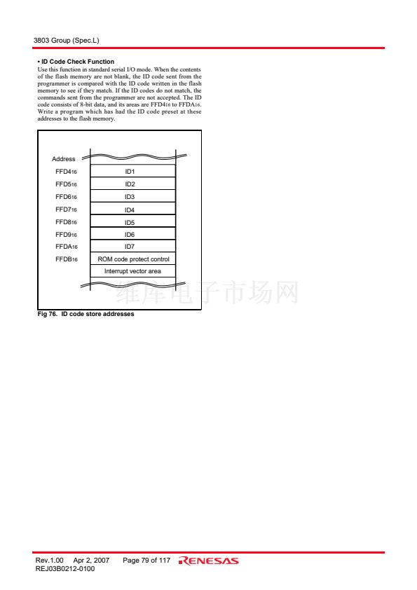
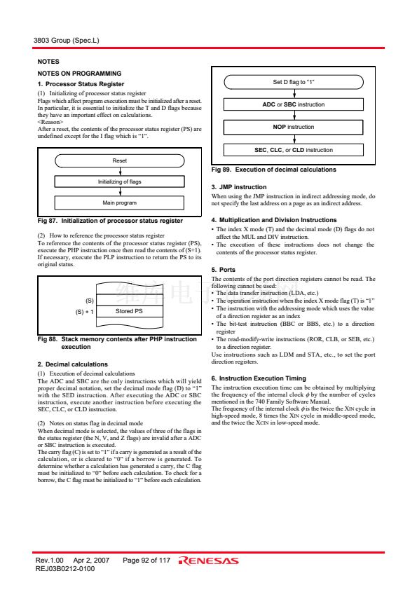
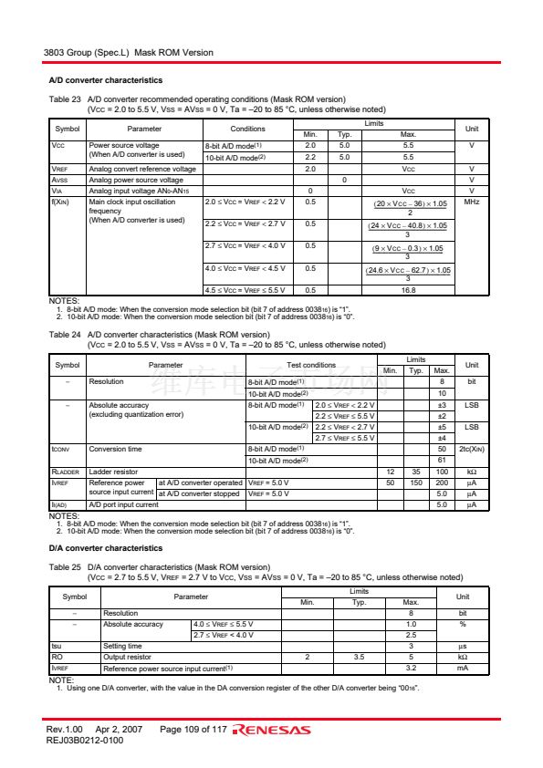
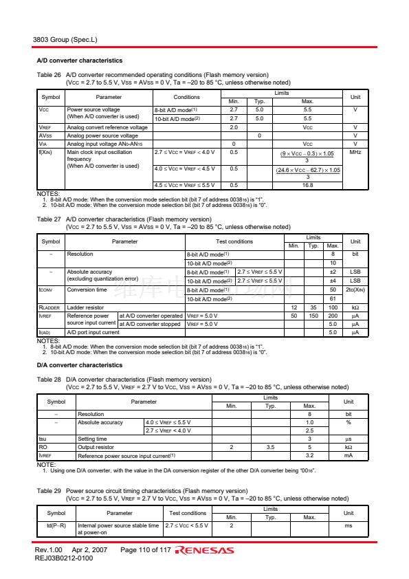
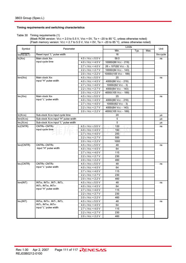
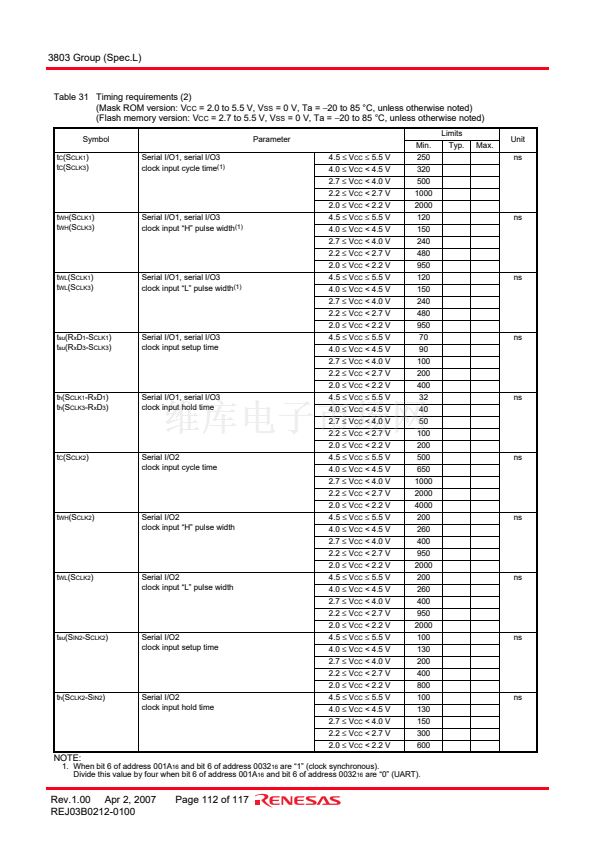
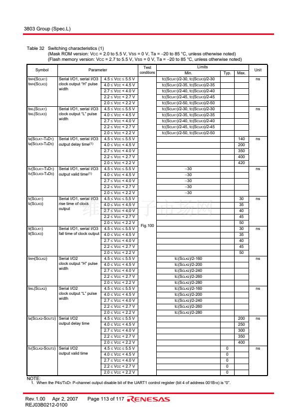
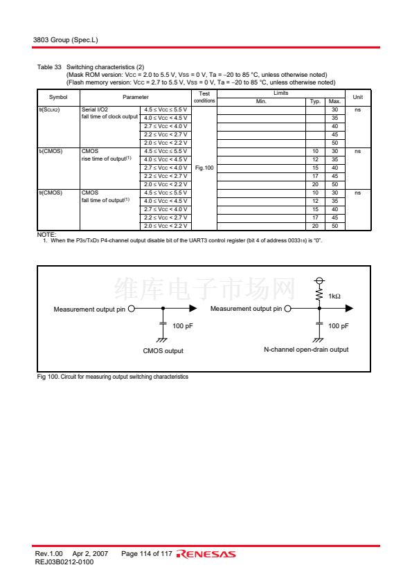
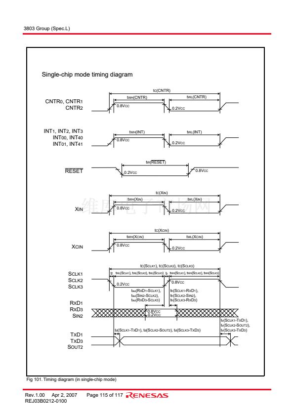
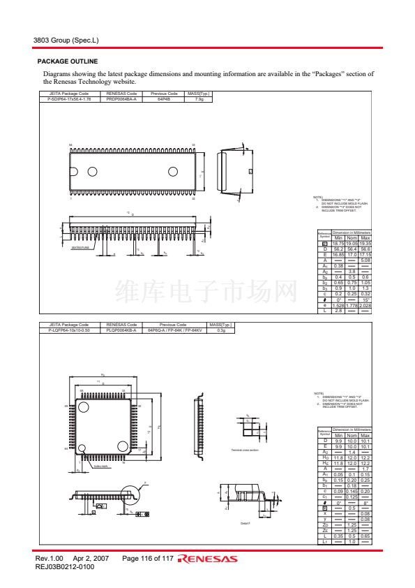
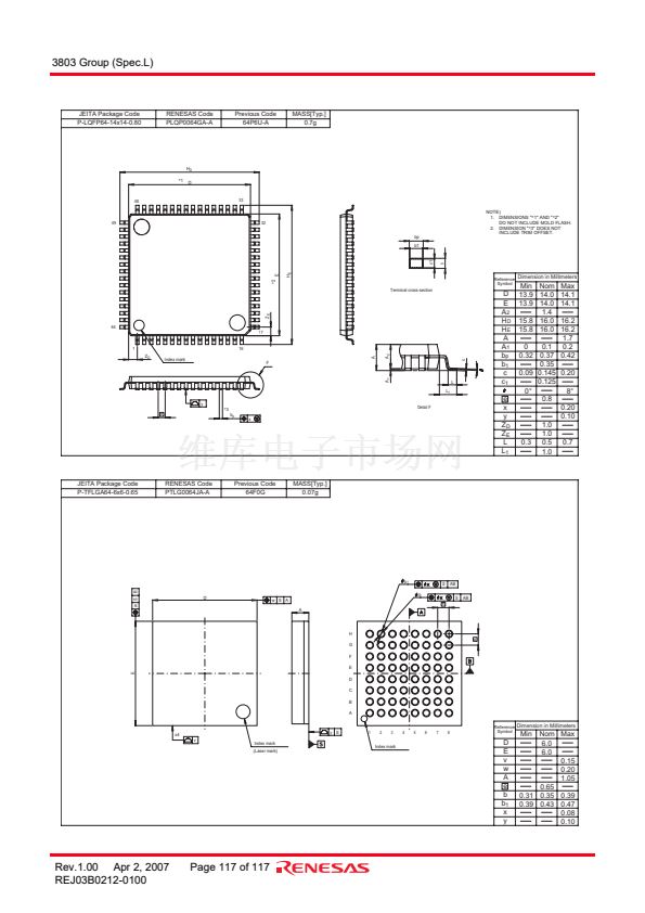
3803 Group (Spec.L)
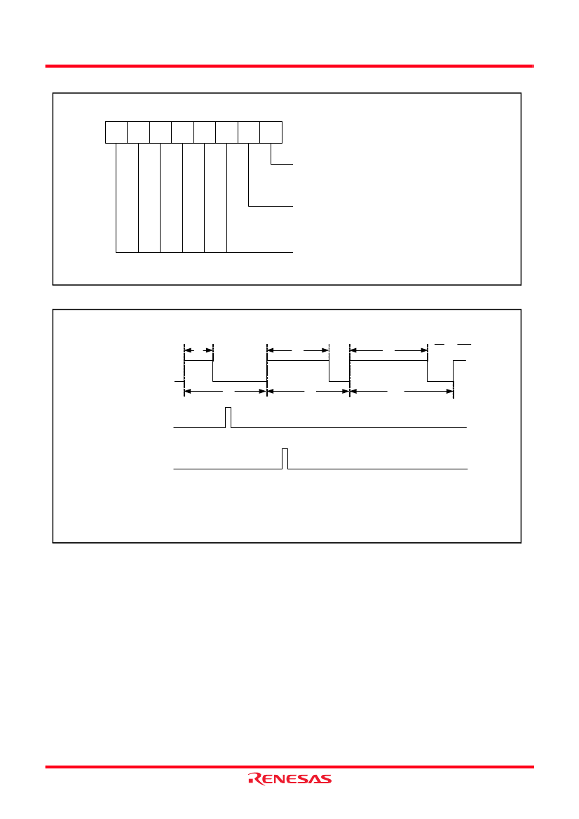
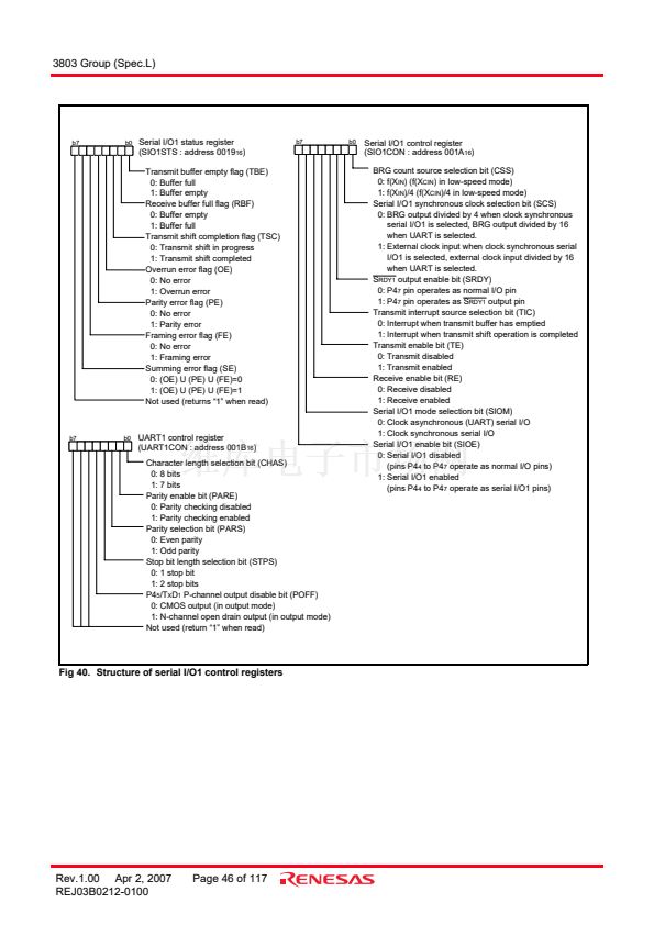
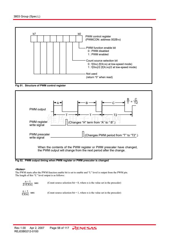
b7
b0
PWM control register
(PWMCON: address 002B
16
)
PWM function enable bit
0 : PWM disabled
1 : PWM enabled
Count source selection bit
0 : f(X
IN
) (f(X
CIN
) at low-speed mode)
1 : f(X
IN
)/2 (f(X
CIN
)/2 at low-speed mode)
Not used
(return 鈥?鈥?when read)
Fig 51. Structure of PWM control register
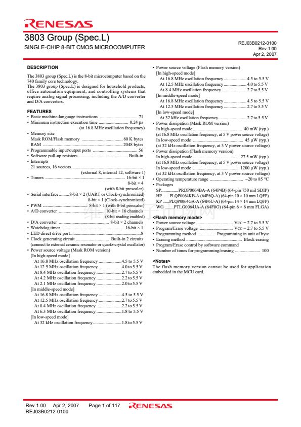
A
PWM output
T
PWM register
write signal
PWM prescaler
write signal
B
C
B
C
= T2
T
T
T2
(Changes 鈥淗鈥?term from 鈥淎鈥?to 鈥?B鈥?)
(Changes PWM period from 鈥淭鈥?to 鈥淭2鈥?)
When the contents of the PWM register or PWM prescaler have changed,
the PWM output will change from the next period after the change.
Fig 52. PWM output timing when PWM register or PWM prescaler is changed
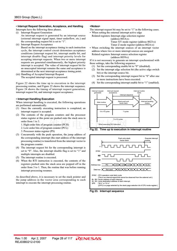
<Notes>
The PWM starts after the PWM function enable bit is set to enable and 鈥淟鈥?level is output from the PWM pin.
The length of this 鈥淟鈥?level output is as follows:
n
+
1
-
----------------------
sec
2
脳
f
(
X
IN
)
n
+
1
---------------
sec
-
f
(
X
IN
)
(Count source selection bit = 0, where n is the value set in the prescaler)
(Count source selection bit = 1, where n is the value set in the prescaler)
Rev.1.00 Apr 2, 2007
REJ03B0212-0100
Page 58 of 117


 1
1
 2
2
 3
3
 4
4
 5
5
 6
6
 7
7
 8
8
 9
9
 10
10
 11
11
 12
12
 13
13
 14
14
 15
15
 16
16
 17
17
 18
18
 19
19
 20
20
 21
21
 22
22
 23
23
 24
24
 25
25
 26
26
 27
27
 28
28
 29
29
 30
30
 31
31
 32
32
 33
33
 34
34
 35
35
 36
36
 37
37
 38
38
 39
39
 40
40
 41
41
 42
42
 43
43
 44
44
 45
45
 46
46
 47
47
 48
48
 49
49
 50
50
 51
51
 52
52
 53
53
 54
54
 55
55
 56
56
 57
57
 58
58
 59
59
 60
60
 61
61
 62
62
 63
63
 64
64
 65
65
 66
66
 67
67
 68
68
 69
69
 70
70
 71
71
 72
72
 73
73
 74
74
 75
75
 76
76
 77
77
 78
78
 79
79
 80
80
 81
81
 82
82
 83
83
 84
84
 85
85
 86
86
 87
87
 88
88
 89
89
 90
90
 91
91
 92
92
 93
93
 94
94
 95
95
 96
96
 97
97
 98
98
 99
99
 100
100
 101
101
 102
102
 103
103
 104
104
 105
105
 106
106
 107
107
 108
108
 109
109
 110
110
 111
111
 112
112
 113
113
 114
114
 115
115
 116
116
 117
117
 118
118
 119
119
