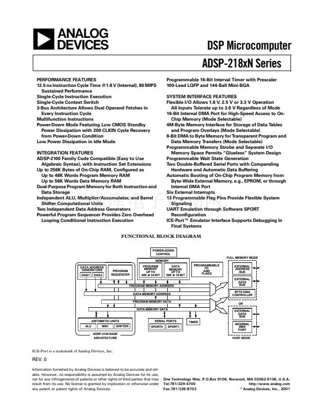
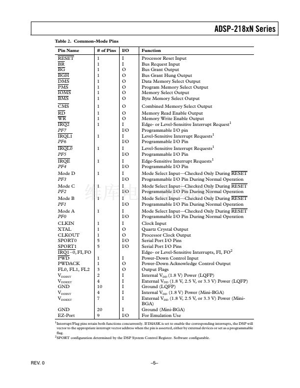
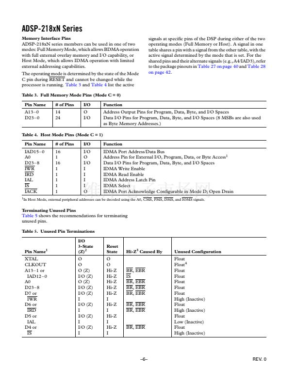
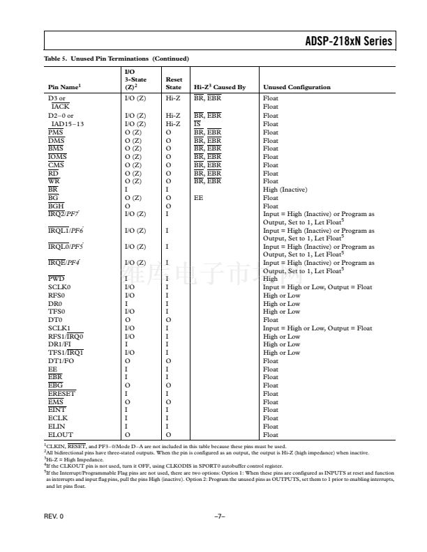
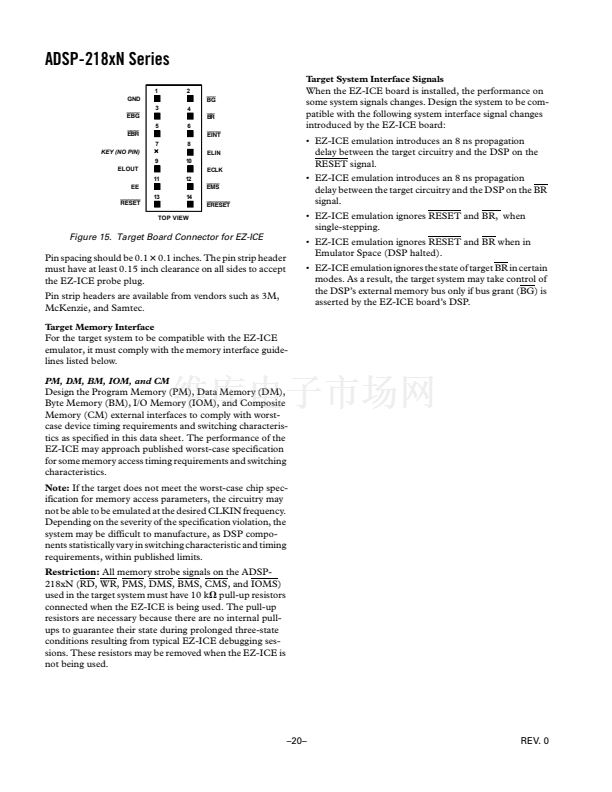
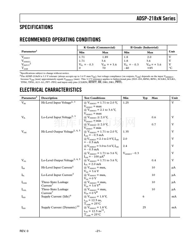
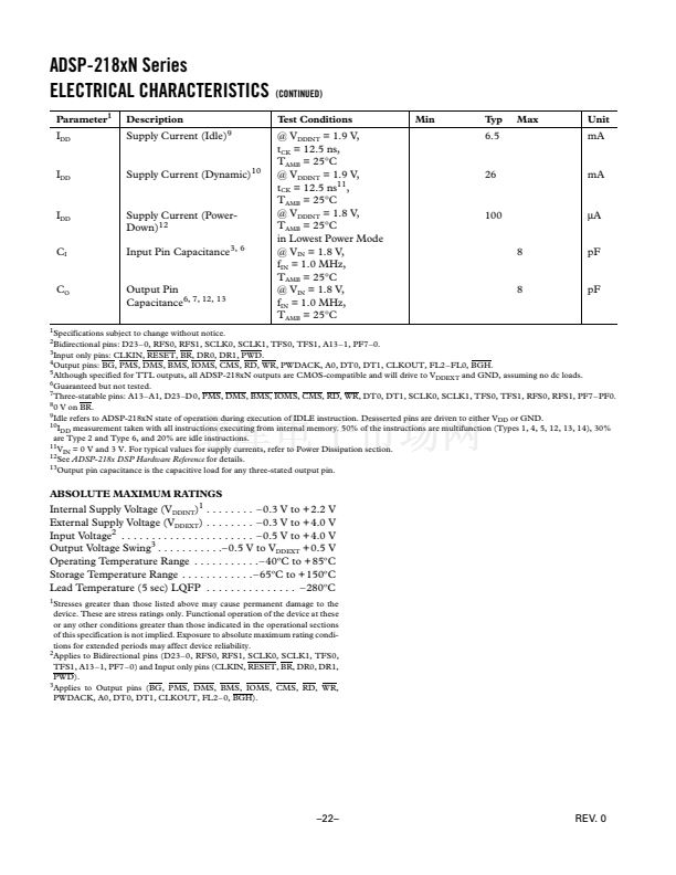
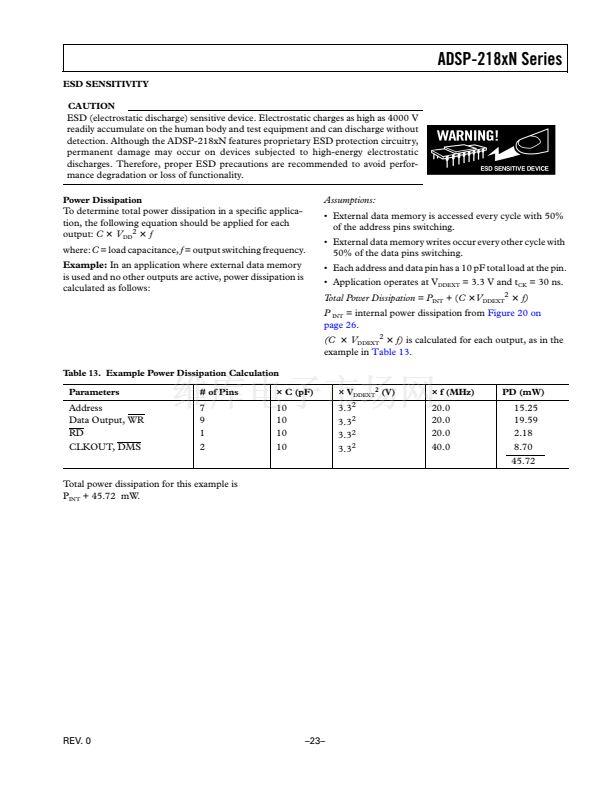
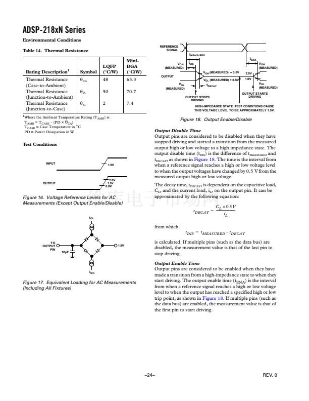
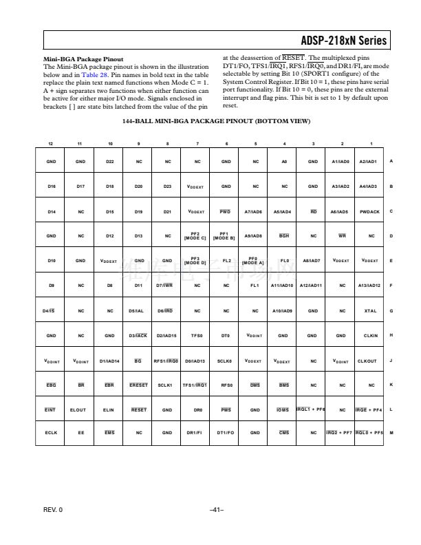
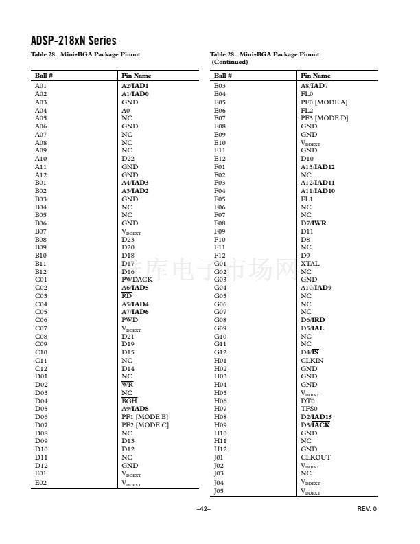
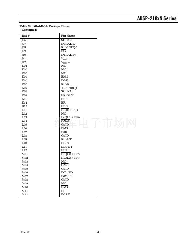
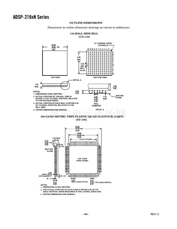
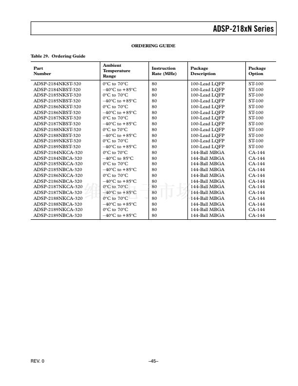
ADSP-218xN Series
Memory-Mapped Registers (New to the ADSP-218xM
and N series)
WAIT STATE CONTROL
15 14 13 12 11 10
1
1
1
1
1
1
9
1
8
1
7
1
6
1
5
1
4
3
ADSP-218xN series members have three memory-mapped
registers that differ from other ADSP-21xx Family DSPs.
The slight modifications to these registers (Wait State Con-
trol, Programmable Flag and Composite Select Control,
and System Control) provide the ADSP-218xN鈥檚 wait state
and BMS control features. Default bit values at reset are
shown; if no value is shown, the bit is undefined at reset.
Reserved bits are shown on a grey field. These bits should
always be written with zeros.
I/O Space (Full Memory Mode)
DWAIT
IOWAIT3
IOWAIT2
WAIT STATE MODE SELECT
ait
0 = NORMAL MODE (PWAIT,
W
DWAIT, IOWAIT0鈥? = N WAIT STATES,
t
RANGING FROM 0 TO
er
7)
Ins
DWAIT, IOWAIT0鈥? = 2N + 1 WAIT STATES,
1 = 2N + 1 MODE (PWAIT,
RANGING FROM 0 TO 15)
on
C
IOWAIT1
te
Sta
l
tro
1
2
er
t
1
g is
1
1
Re
1
0
1
DM(0X3FFE)
IOWAIT0
Figure 9. Wait State Control Register
Composite Memory Select
ADSP-218xN series members support an additional exter-
nal memory space called I/O space. This space is designed
to support simple connections to peripherals (such as data
converters and external registers) or to bus interface ASIC
data registers. I/O space supports 2048 locations of 16-bit
wide data. The lower eleven bits of the external address bus
are used; the upper three bits are undefined.
Two instructions were added to the core ADSP-2100
Family instruction set to read from and write to I/O memory
space. The I/O space also has four dedicated three-bit wait
state registers, IOWAIT0鈥? as shown in
Figure 9,
which in
combination with the wait state mode bit, specify up to 15
wait states to be automatically generated for each of four
regions. The wait states act on address ranges, as shown
in
Table 10.
Note:
In Full Memory Mode, all 2048 locations of I/O space
are directly addressable. In Host Memory Mode, only
address pin A0 is available; therefore, additional logic is
required externally to achieve complete addressability of the
2048 I/O space locations.
Table 10. Wait States
Address Range
Wait State Register
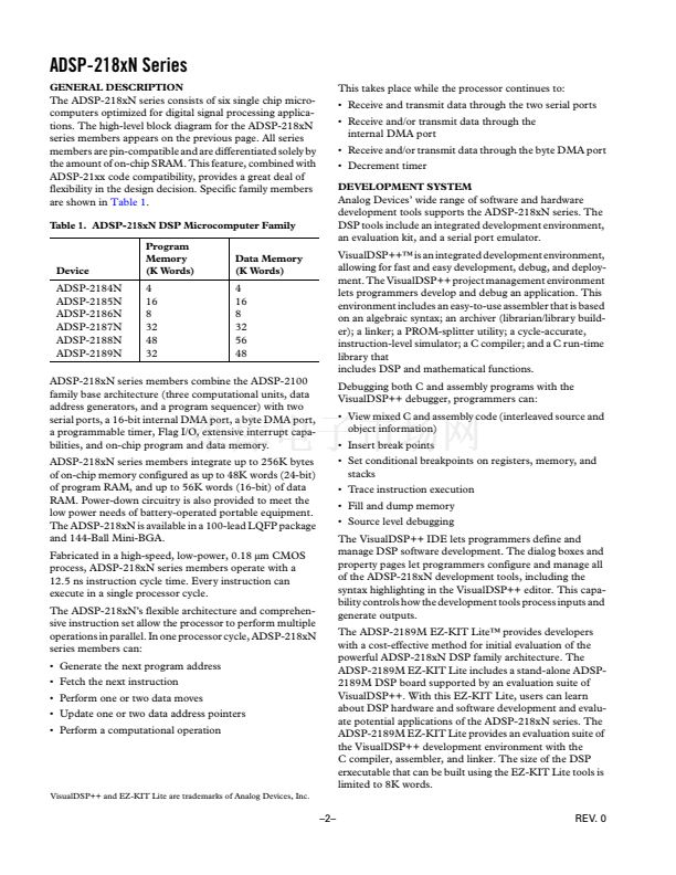
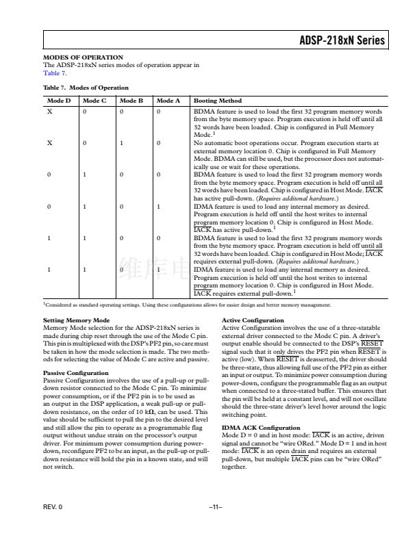
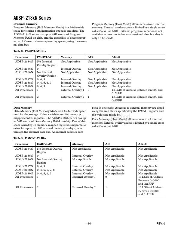
ADSP-218xN series members have a programmable
memory select signal that is useful for generating memory
select signals for memories mapped to more than one space.
The CMS signal is generated to have the same timing as
each of the individual memory select signals (PMS, DMS,
BMS, IOMS) but can combine their functionality. Each bit
in the CMSSEL register, when set, causes the CMS signal
to be asserted when the selected memory select is asserted.
For example, to use a 32K word memory to act as both
program and data memory, set the PMS and DMS bits in
the CMSSEL register and use the CMS pin to drive the chip
select of the memory, and use either DMS or PMS as the
additional address bit.
The CMS pin functions like the other memory select signals
with the same timing and bus request logic. A 1 in the enable
bit causes the assertion of the CMS signal at the same time
as the selected memory select signal. All enable bits default
to 1 at reset, except the BMS bit.
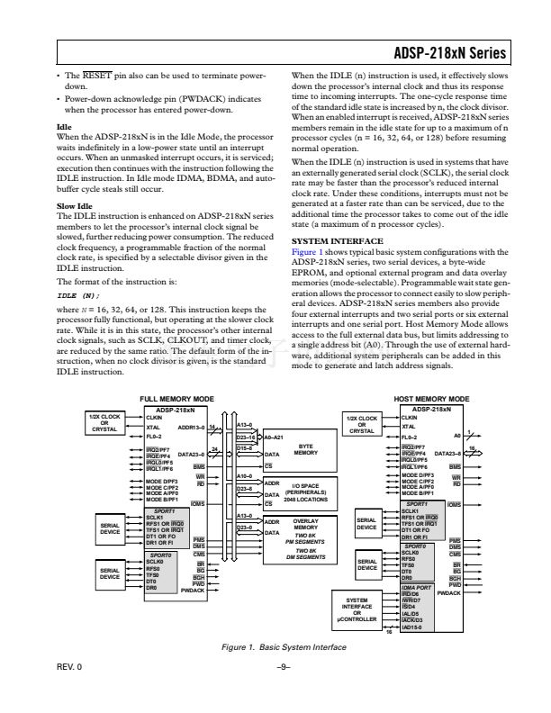
See
Figure 10
and
Figure 11
for illustration of the program-
mable flag and composite control register and the system
control register.
0x000鈥?x1FF
0x200鈥?x3FF
0x400鈥?x5FF
0x600鈥?x7FF
IOWAIT0 and Wait State Mode
Select Bit
IOWAIT1 and Wait State Mode
Select Bit
IOWAIT2 and Wait State Mode
Select Bit
IOWAIT3 and Wait State Mode
Select Bit
PROGRAMMABLE FLAG AND COMPOSITE
SELECT CONTROL
15 14
1
1
13 12
1
1
11 10
1
0
9
1
8
1
7
0
6
0
5
0
4
0
3
0
2
0
1
0
0
0
DM(0X3FE6)
BM W A IT
CM SSEL
0 = D IS A B L E
CMS
1 = E N A B L E
CMS
PFT YP E
0 = IN PU T
1 = O UTPUT
( W H E R E B IT : 1 1 - I O M , 1 0 - B M , 9 - D M , 8 - P M )
Figure 10. Programmable Flag and Composite Control
Register
REV. 0
鈥?5鈥?/div>
prev
next


 1
1
 2
2
 3
3
 4
4
 5
5
 6
6
 7
7
 8
8
 9
9
 10
10
 11
11
 12
12
 13
13
 14
14
 15
15
 16
16
 17
17
 18
18
 19
19
 20
20
 21
21
 22
22
 23
23
 24
24
 25
25
 26
26
 27
27
 28
28
 29
29
 30
30
 31
31
 32
32
 33
33
 34
34
 35
35
 36
36
 37
37
 38
38
 39
39
 40
40
 41
41
 42
42
 43
43
 44
44
 45
45
 46
46
 47
47
 48
48
