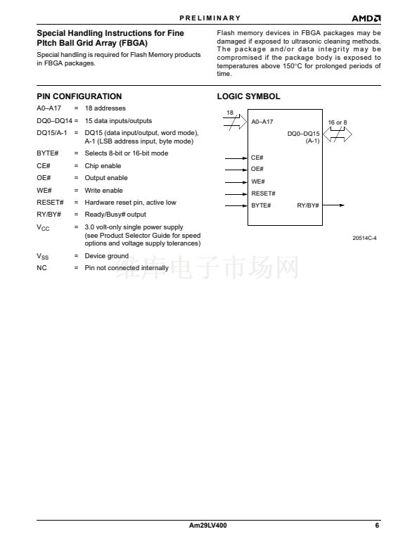
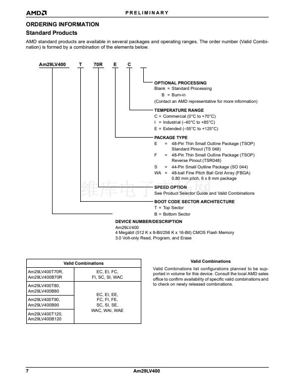
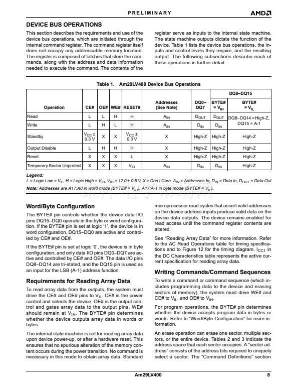
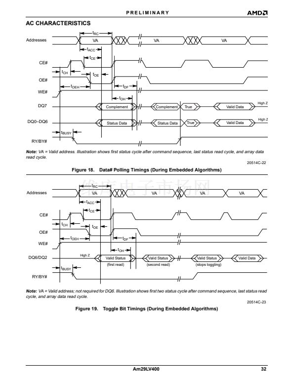
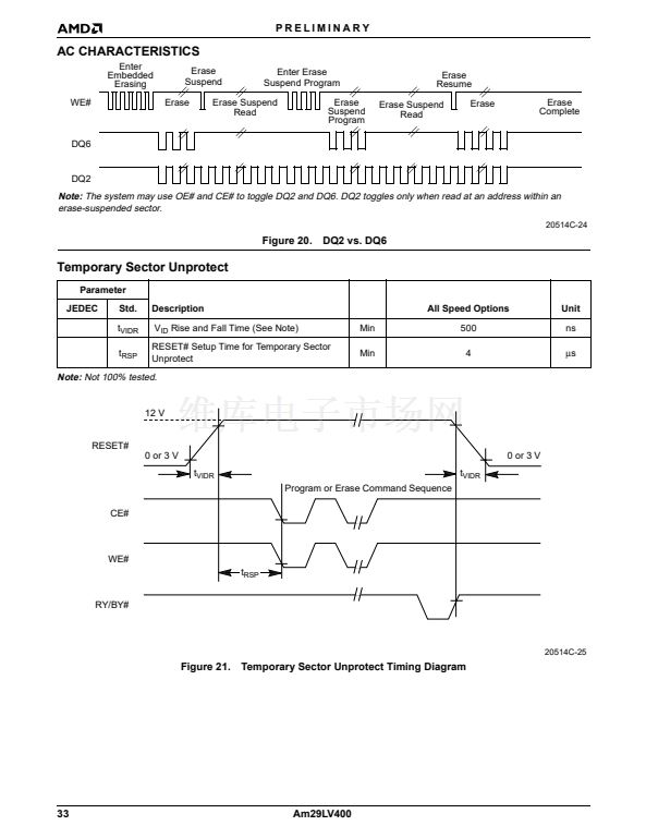
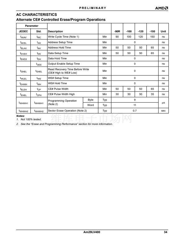
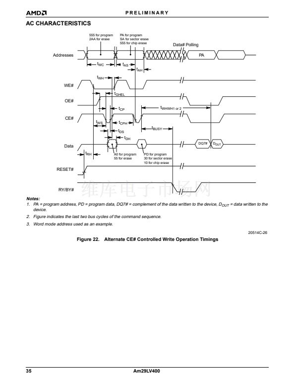
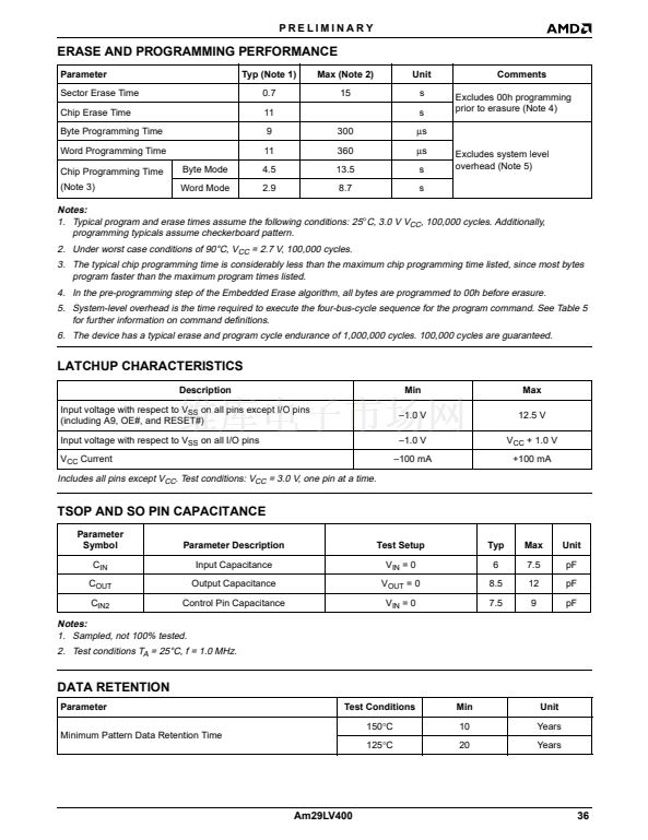
PRELIMINARY
against inadvertent writes (refer to Table 5 for com-
mand definitions). In addition, the following hardware
data protection measures prevent accidental erasure
or programming, which might otherwise be caused by
spurious system level signals during V
CC
power-up
and power-down transitions, or from system noise.
Low V
CC
Write Inhibit
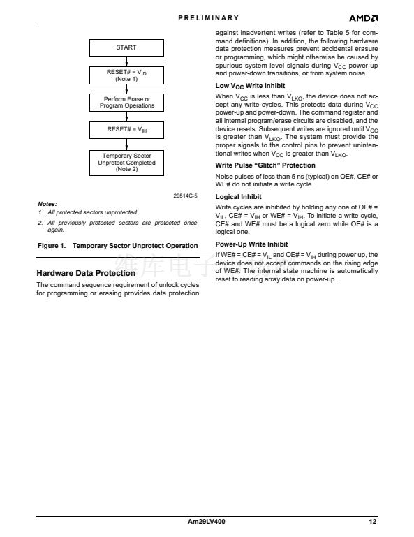
Perform Erase or
Program Operations
START
RESET# = V
ID
(Note 1)
RESET# = V
IH
Temporary Sector
Unprotect Completed
(Note 2)
When V
CC
is less than V
LKO
, the device does not ac-
cept any write cycles. This protects data during V
CC
power-up and power-down. The command register and
all internal program/erase circuits are disabled, and the
device resets. Subsequent writes are ignored until V
CC
is greater than V
LKO
. The system must provide the
proper signals to the control pins to prevent uninten-
tional writes when V
CC
is greater than V
LKO
.
Write Pulse 鈥淕litch鈥?Protection
Noise pulses of less than 5 ns (typical) on OE#, CE# or
WE# do not initiate a write cycle.
20514C-5
Logical Inhibit
Write cycles are inhibited by holding any one of OE# =
V
IL
, CE# = V
IH
or WE# = V
IH
. To initiate a write cycle,
CE# and WE# must be a logical zero while OE# is a
logical one.
Power-Up Write Inhibit
If WE# = CE# = V
IL
and OE# = V
IH
during power up, the
device does not accept commands on the rising edge
of WE#. The internal state machine is automatically
reset to reading array data on power-up.
Notes:
1. All protected sectors unprotected.
2. All previously protected sectors are protected once
again.
Figure 1.
Temporary Sector Unprotect Operation
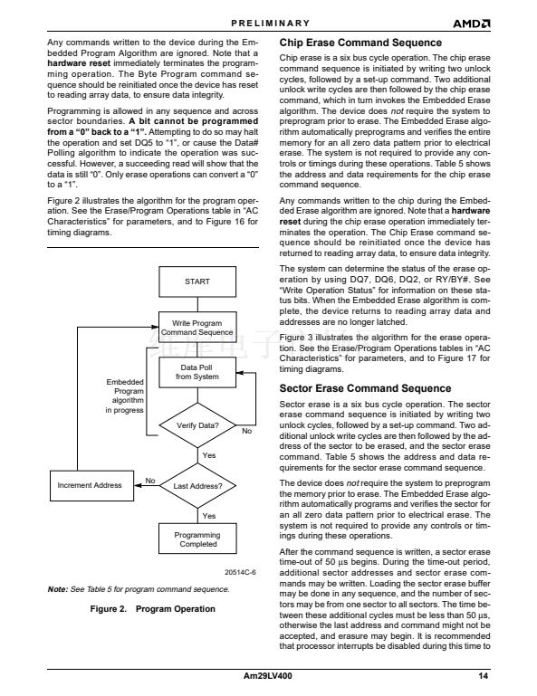
Hardware Data Protection
The command sequence requirement of unlock cycles
for programming or erasing provides data protection
Am29LV400
12


 1
1
 2
2
 3
3
 4
4
 5
5
 6
6
 7
7
 8
8
 9
9
 10
10
 11
11
 12
12
 13
13
 14
14
 15
15
 16
16
 17
17
 18
18
 19
19
 20
20
 21
21
 22
22
 23
23
 24
24
 25
25
 26
26
 27
27
 28
28
 29
29
 30
30
 31
31
 32
32
 33
33
 34
34
 35
35
 36
36
 37
37
 38
38
 39
39
 40
40
