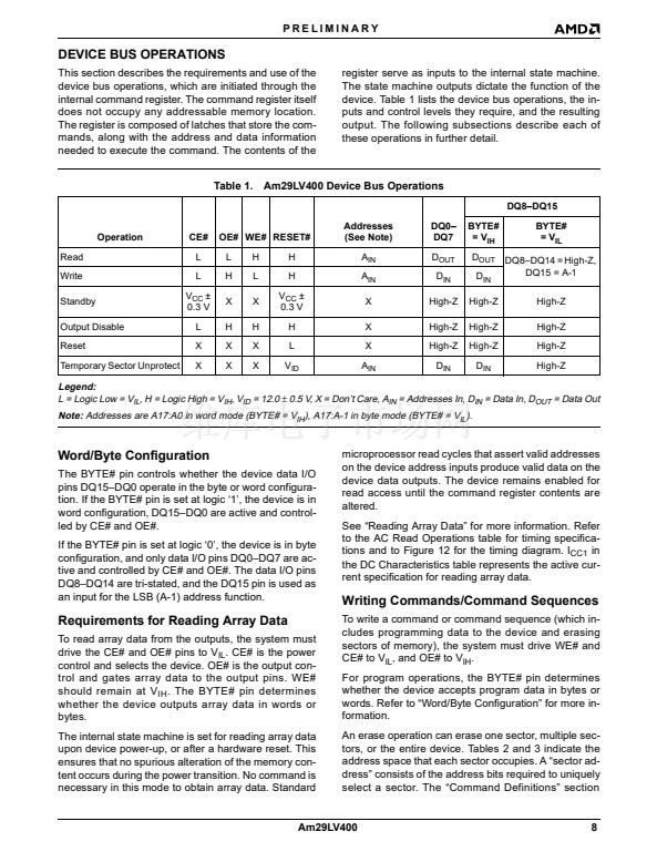
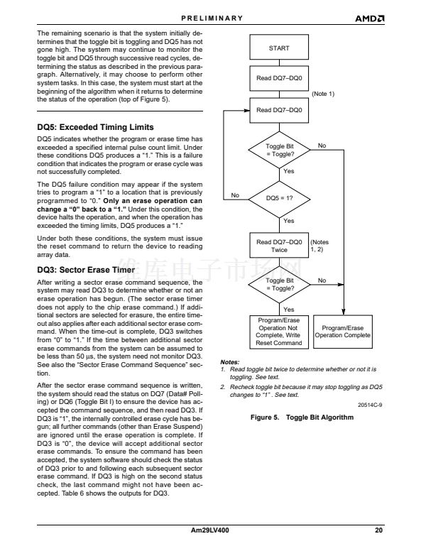
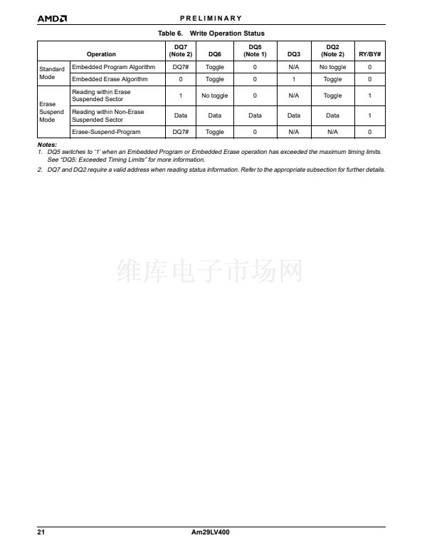
internal command register. The command register itself
does not occupy any addressable memory location.
needed to execute the command. The contents of the
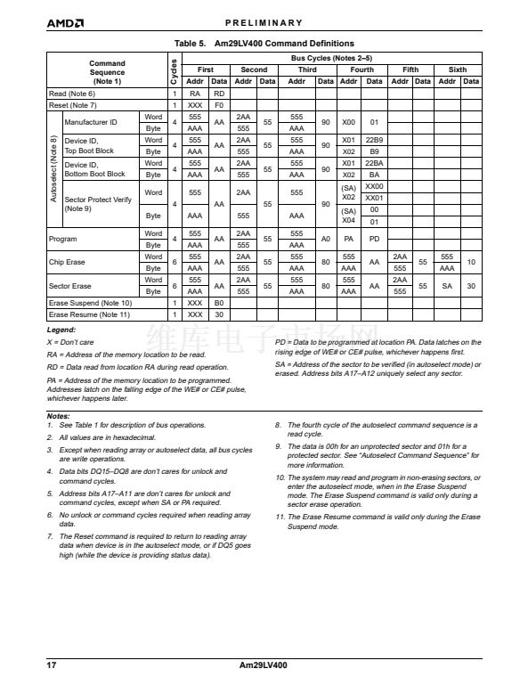
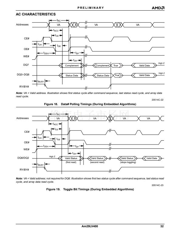
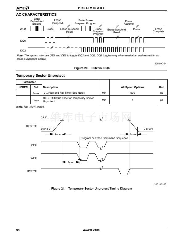
Table 1.
register serve as inputs to the internal state machine.
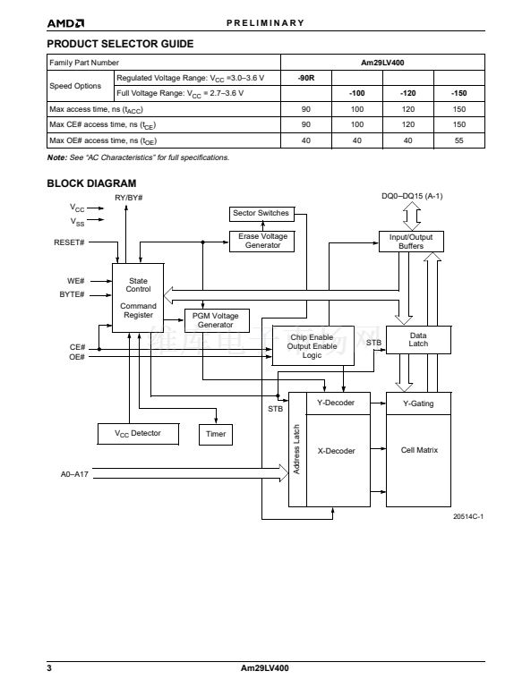
device. Table 1 lists the device bus operations, the in-
output. The following subsections describe each of
these operations in further detail.
DQ0鈥?/div>
DQ7
D
OUT
D
IN
High-Z
High-Z
High-Z
D
IN
BYTE#
= V
IH
D
OUT
D
IN
High-Z
High-Z
High-Z
D
IN
BYTE#
= V
IL
DQ8鈥揇Q14 = High-Z,
DQ15 = A-1
High-Z
High-Z
High-Z
High-Z
Legend:
L = Logic Low = V
IL
, H = Logic High = V
IH
, V
ID
= 12.0
卤
0.5 V, X = Don鈥檛 Care, A
IN
= Addresses In, D
IN
= Data In, D
OUT
= Data Out
Note:
Addresses are A17:A0 in word mode (BYTE# = V
IH
), A17:A-1 in byte mode (BYTE# = V
IL
).
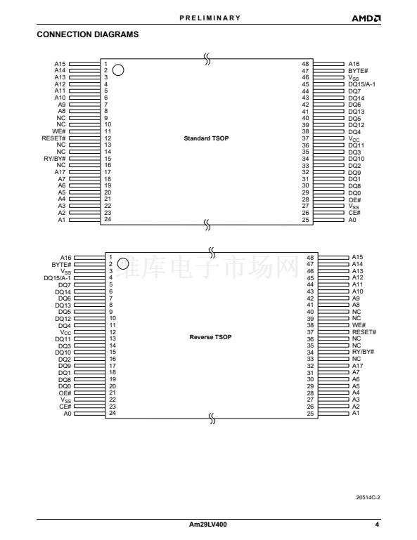
Word/Byte Configuration
The BYTE# pin controls whether the device data I/O
pins DQ15鈥揇Q0 operate in the byte or word configura-
tion. If the BYTE# pin is set at logic 鈥?鈥? the device is in
word configuration, DQ15鈥揇Q0 are active and control-
led by CE# and OE#.
If the BYTE# pin is set at logic 鈥?鈥? the device is in byte
configuration, and only data I/O pins DQ0鈥揇Q7 are ac-
tive and controlled by CE# and OE#. The data I/O pins
DQ8鈥揇Q14 are tri-stated, and the DQ15 pin is used as
an input for the LSB (A-1) address function.
microprocessor read cycles that assert valid addresses
on the device address inputs produce valid data on the
device data outputs. The device remains enabled for
read access until the command register contents are
altered.
See 鈥淩eading Array Data鈥?for more information. Refer
to the AC Read Operations table for timing specifica-
tions and to Figure 12 for the timing diagram. I
CC1
in
the DC Characteristics table represents the active cur-
rent specification for reading array data.
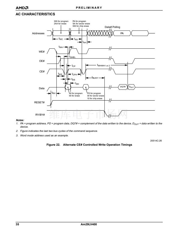
Writing Commands/Command Sequences
To write a command or command sequence (which in-
cludes programming data to the device and erasing
sectors of memory), the system must drive WE# and
CE# to V
IL
, and OE# to V
IH
.
For program operations, the BYTE# pin determines
whether the device accepts program data in bytes or
words. Refer to 鈥淲ord/Byte Configuration鈥?for more in-
formation.
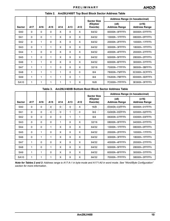
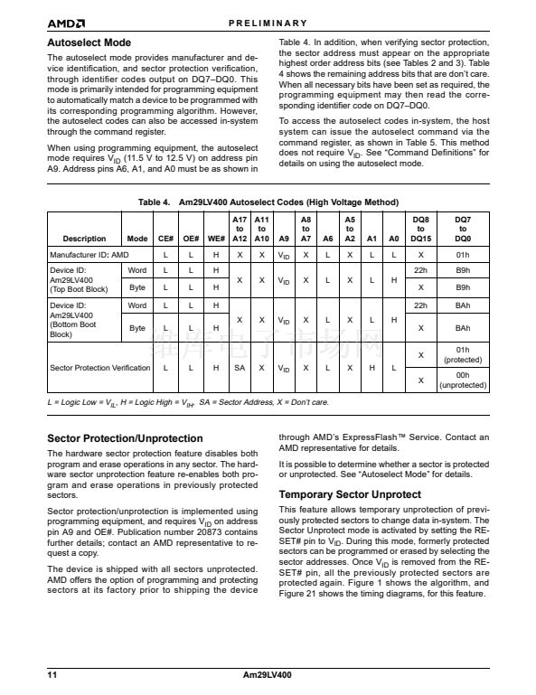
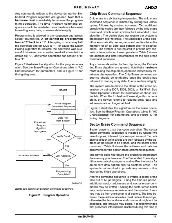
An erase operation can erase one sector, multiple sec-
tors, or the entire device. Tables 2 and 3 indicate the
address space that each sector occupies. A 鈥渟ector ad-
dress鈥?consists of the address bits required to uniquely
select a sector. The 鈥淐ommand Definitions鈥?section
Requirements for Reading Array Data
To read array data from the outputs, the system must
drive the CE# and OE# pins to V
IL
. CE# is the power
control and selects the device. OE# is the output con-
trol and gates array data to the output pins. WE#
should remain at V
IH
. The BYTE# pin determines
whether the device outputs array data in words or
bytes.
The internal state machine is set for reading array data
upon device power-up, or after a hardware reset. This
ensures that no spurious alteration of the memory con-
tent occurs during the power transition. No command is
necessary in this mode to obtain array data. Standard
Am29LV400
8


 1
1
 2
2
 3
3
 4
4
 5
5
 6
6
 7
7
 8
8
 9
9
 10
10
 11
11
 12
12
 13
13
 14
14
 15
15
 16
16
 17
17
 18
18
 19
19
 20
20
 21
21
 22
22
 23
23
 24
24
 25
25
 26
26
 27
27
 28
28
 29
29
 30
30
 31
31
 32
32
 33
33
 34
34
 35
35
 36
36
 37
37
 38
38
 39
39
 40
40
