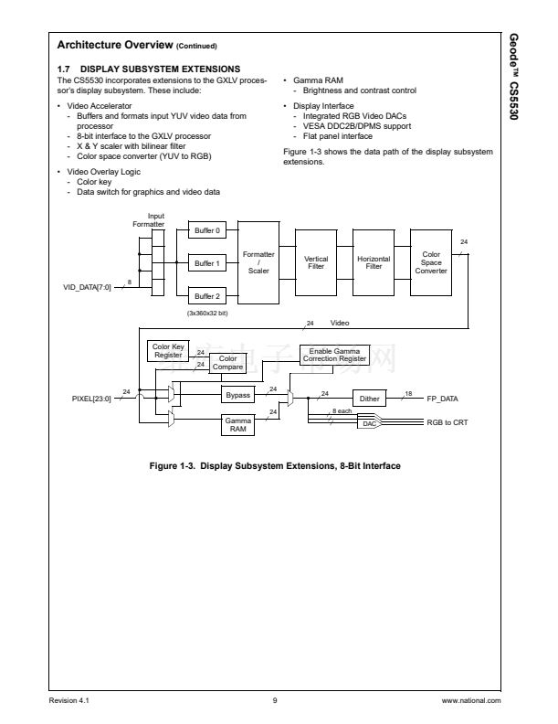
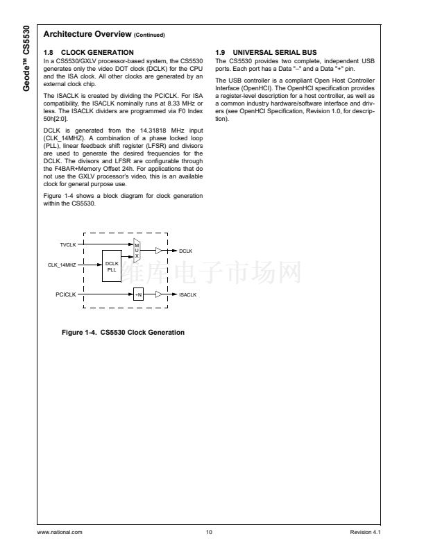
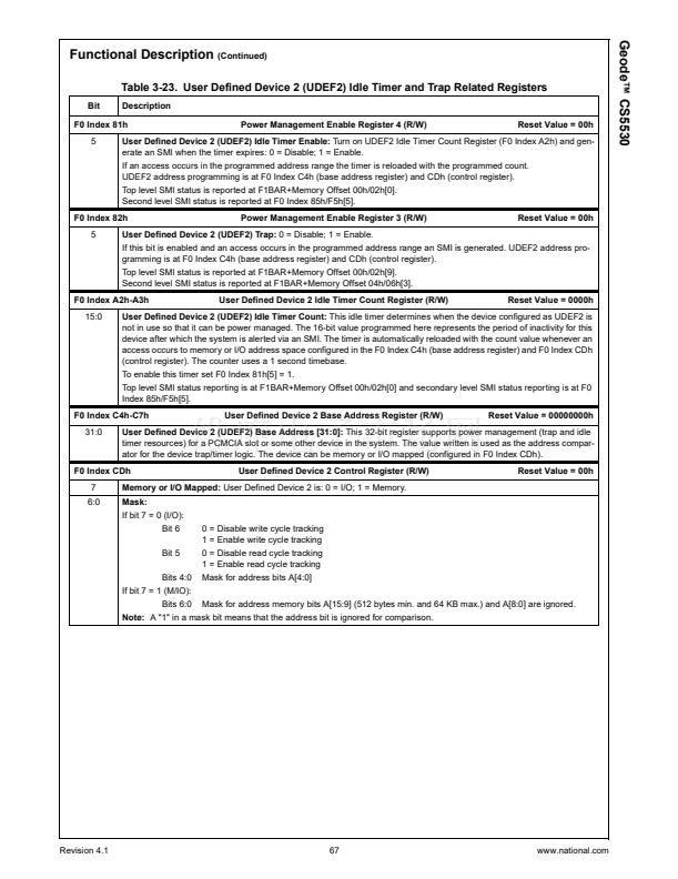
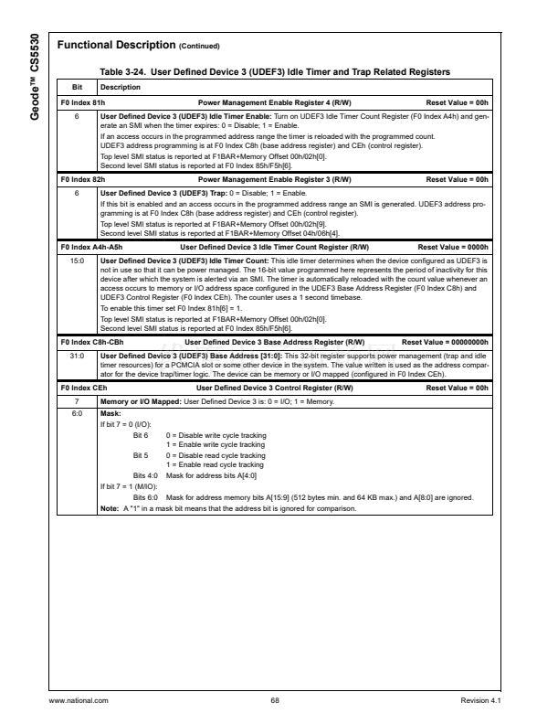
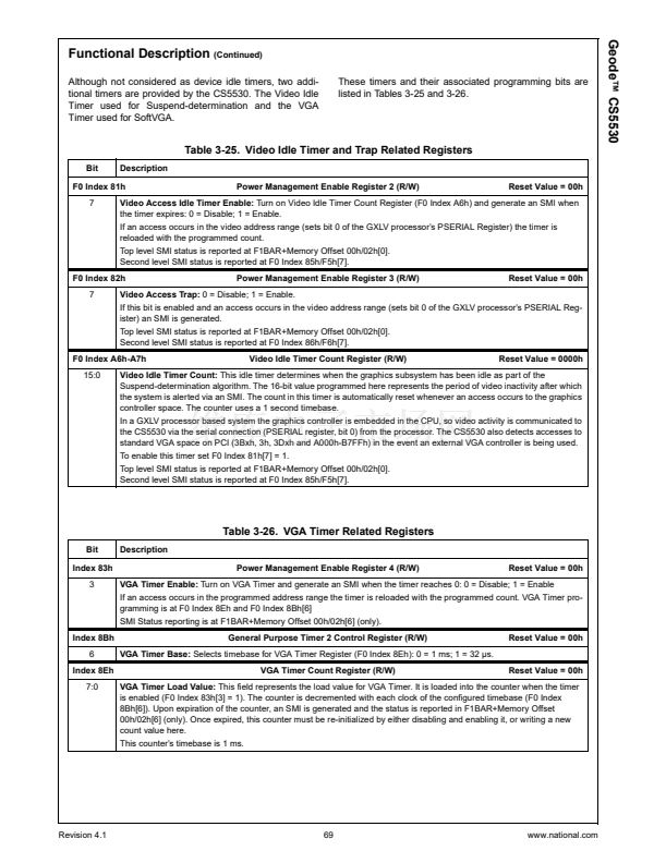
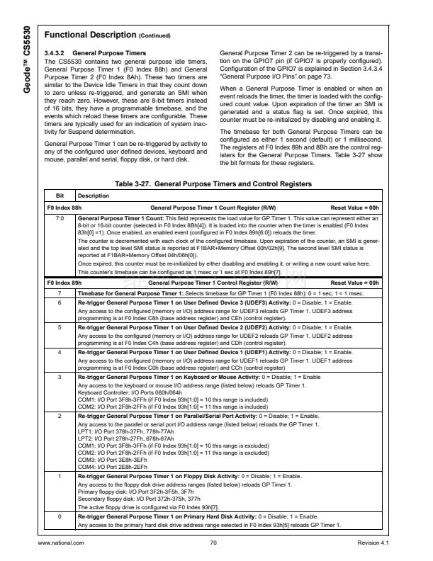
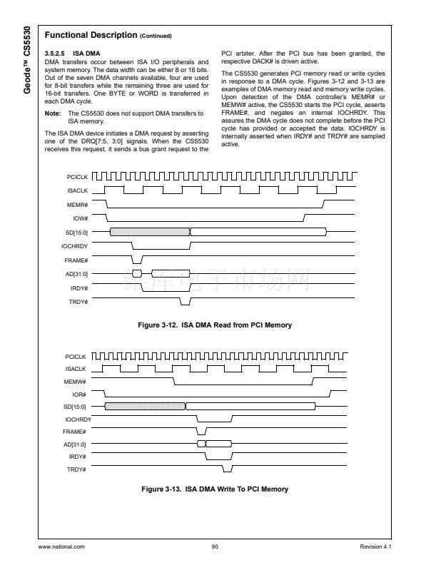
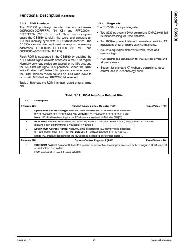
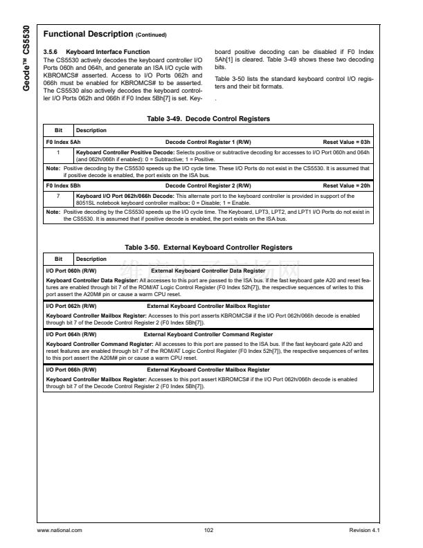
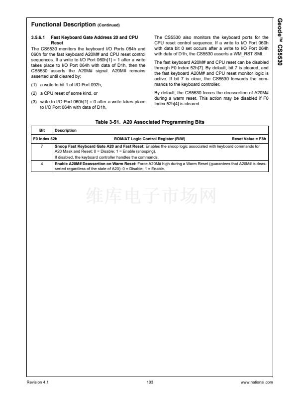
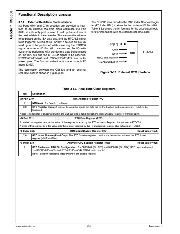
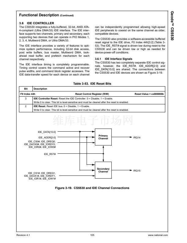
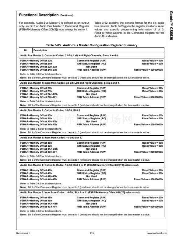
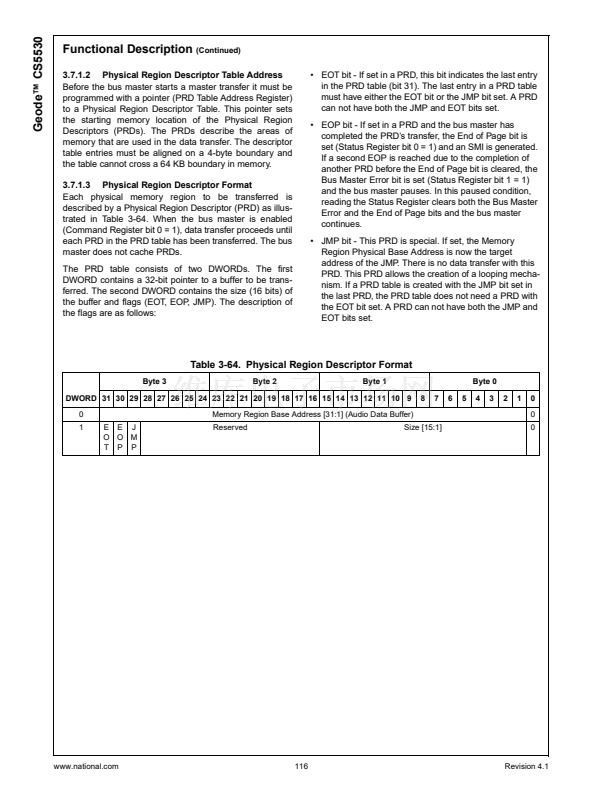
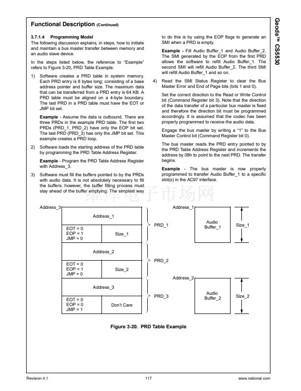
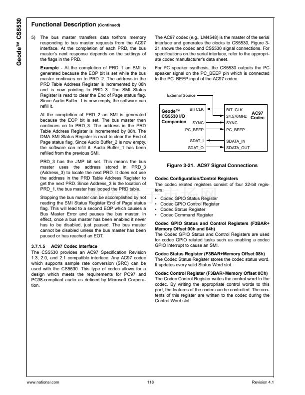
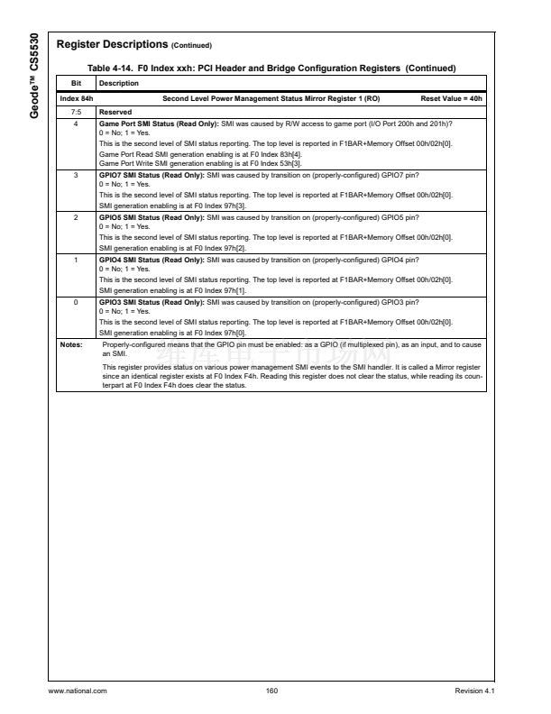
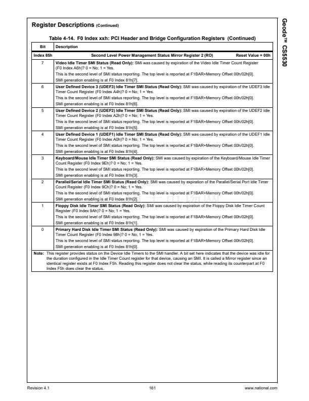
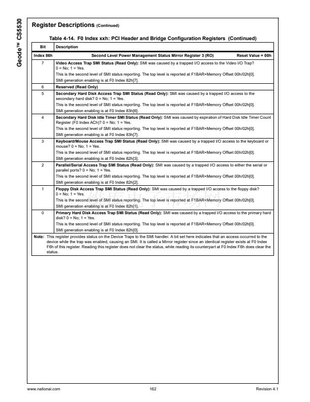
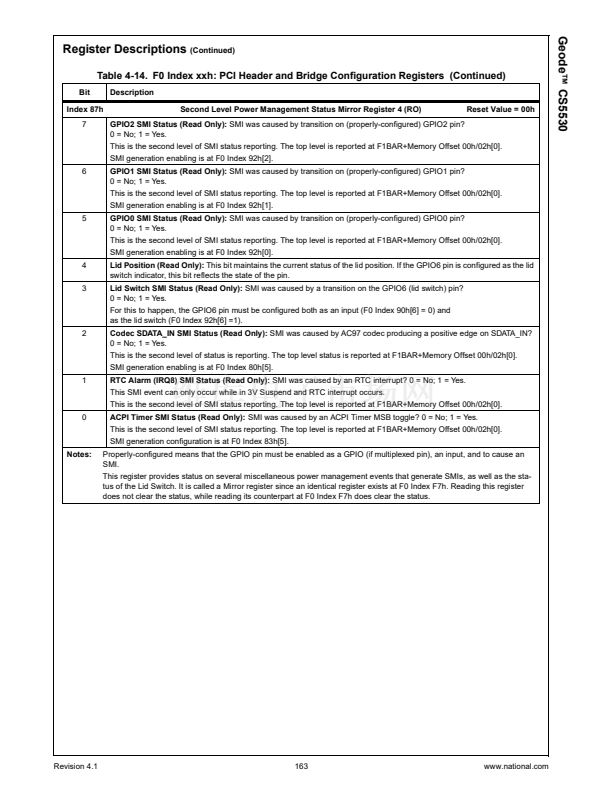
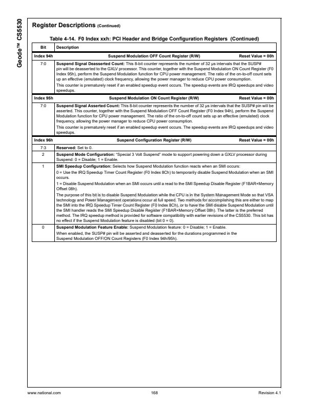
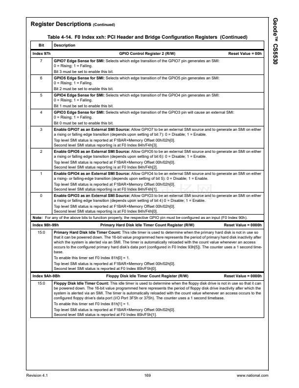
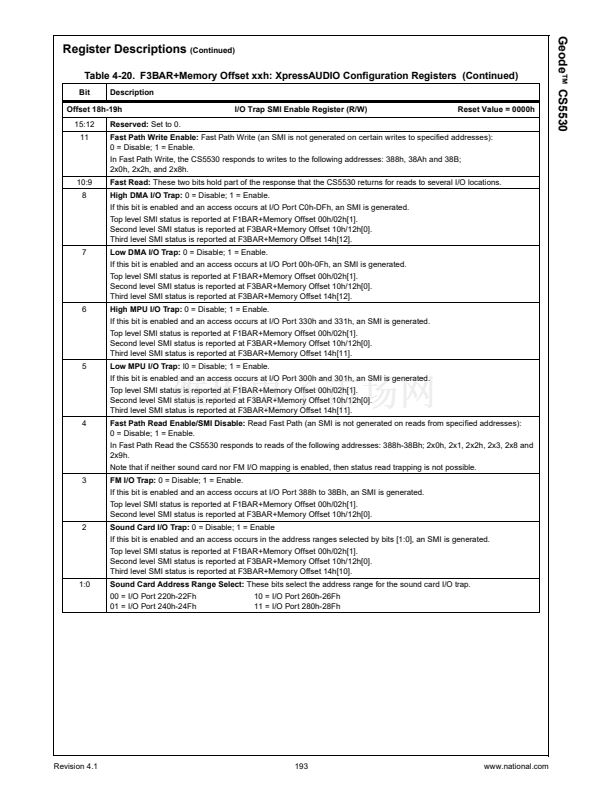
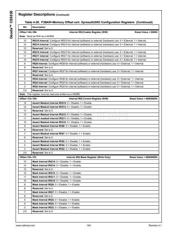
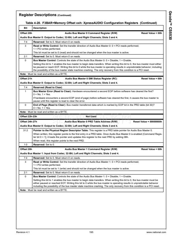
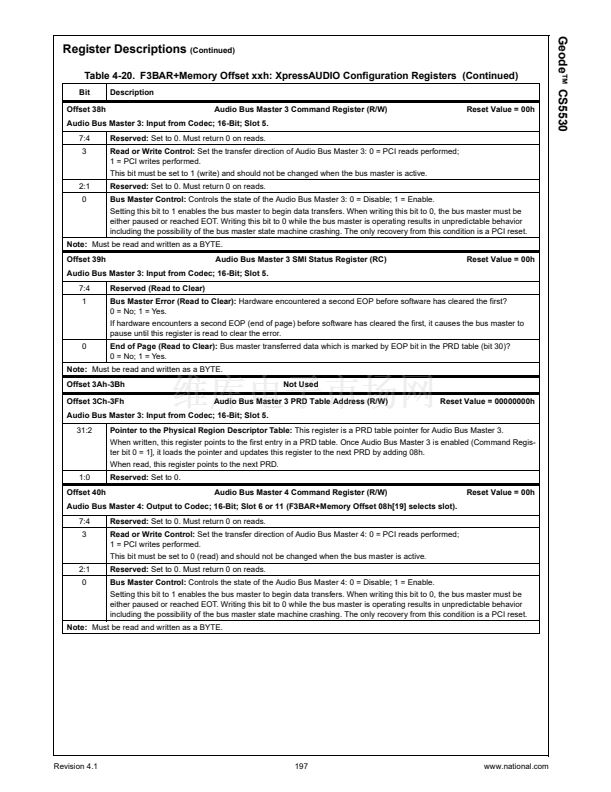
Geode鈩?CS5530
Signal Definitions
(Continued)
2.2
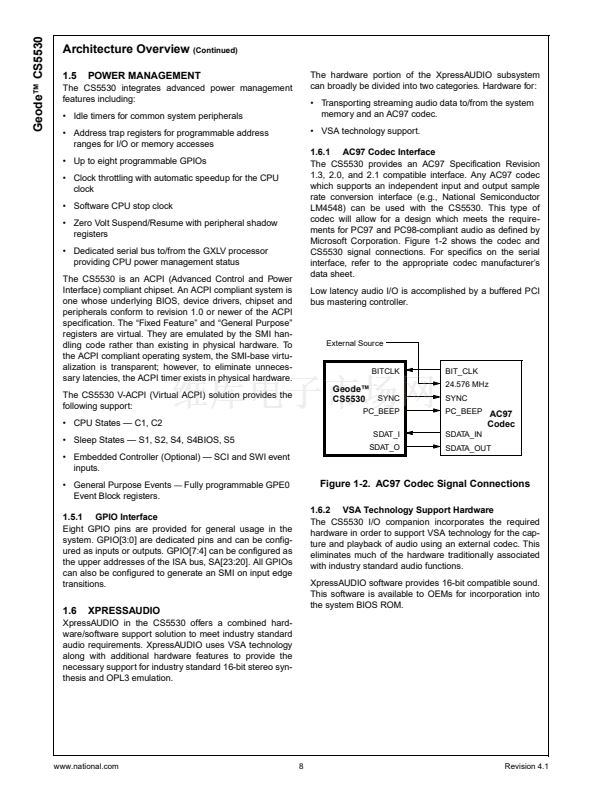
2.2.1
SIGNAL DESCRIPTIONS
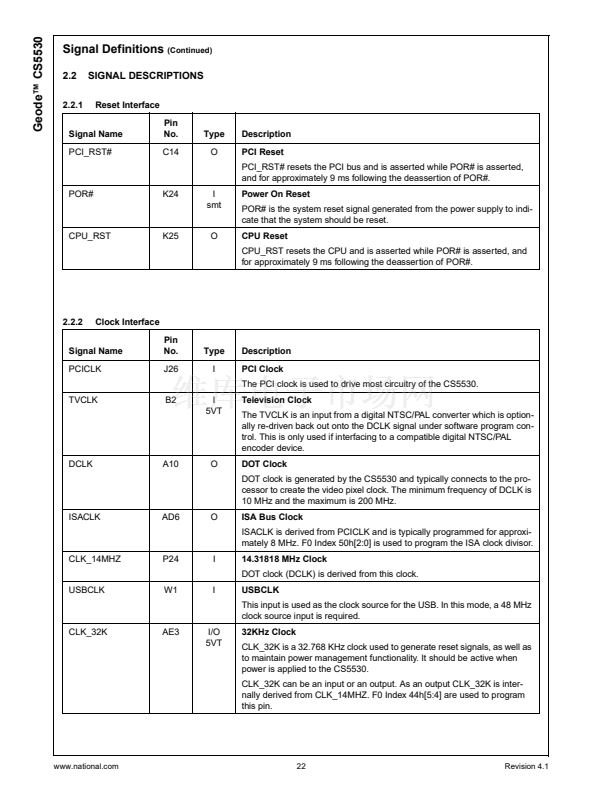
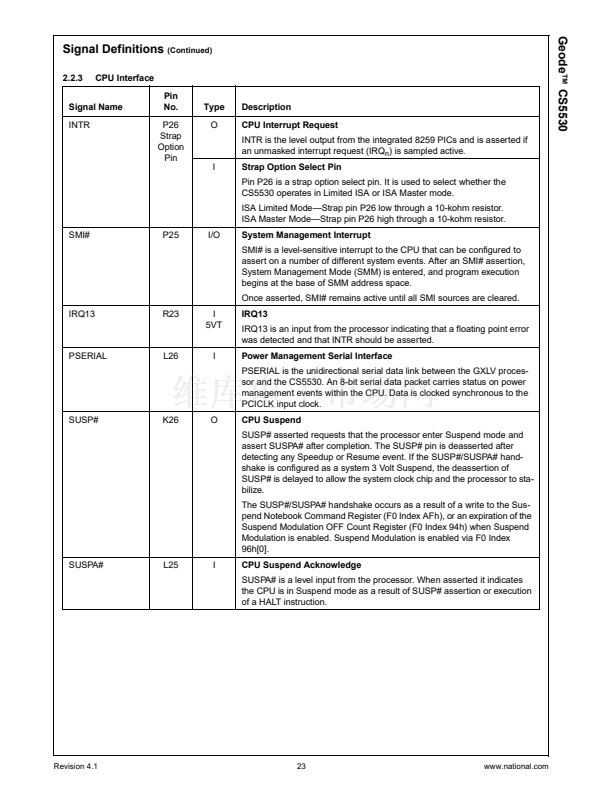
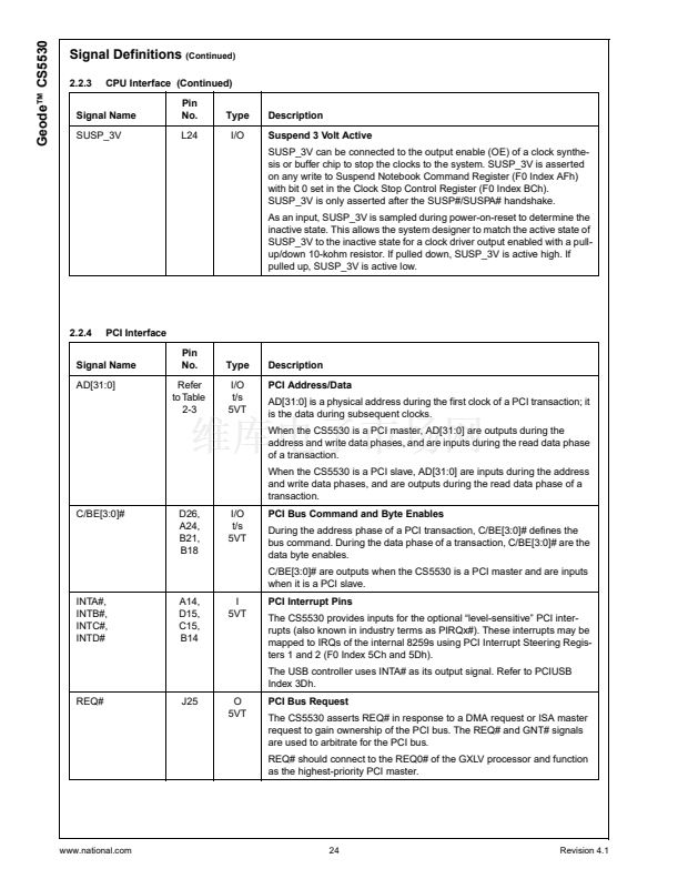
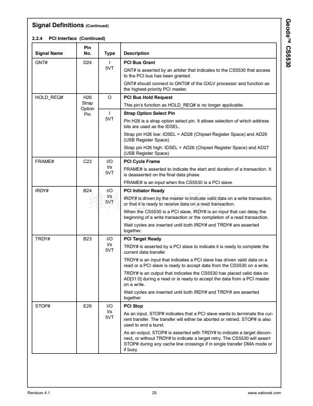
Reset Interface
Pin
No.
C14
Type
O
Description
PCI Reset
PCI_RST# resets the PCI bus and is asserted while POR# is asserted,
and for approximately 9 ms following the deassertion of POR#.
Signal Name
PCI_RST#
POR#
K24
I
smt
Power On Reset
POR# is the system reset signal generated from the power supply to indi-
cate that the system should be reset.
CPU Reset
CPU_RST resets the CPU and is asserted while POR# is asserted, and
for approximately 9 ms following the deassertion of POR#.
CPU_RST
K25
O
2.2.2
Clock Interface
Pin
No.
J26
Type
I
Description
PCI Clock
The PCI clock is used to drive most circuitry of the CS5530.
Signal Name
PCICLK
TVCLK
B2
I
5VT
Television Clock
The TVCLK is an input from a digital NTSC/PAL converter which is option-
ally re-driven back out onto the DCLK signal under software program con-
trol. This is only used if interfacing to a compatible digital NTSC/PAL
encoder device.
DOT Clock
DOT clock is generated by the CS5530 and typically connects to the pro-
cessor to create the video pixel clock. The minimum frequency of DCLK is
10 MHz and the maximum is 200 MHz.
DCLK
A10
O
ISACLK
AD6
O
ISA Bus Clock
ISACLK is derived from PCICLK and is typically programmed for approxi-
mately 8 MHz. F0 Index 50h[2:0] is used to program the ISA clock divisor.
CLK_14MHZ
P24
I
14.31818 MHz Clock
DOT clock (DCLK) is derived from this clock.
USBCLK
W1
I
USBCLK
This input is used as the clock source for the USB. In this mode, a 48 MHz
clock source input is required.
CLK_32K
AE3
I/O
5VT
32KHz Clock
CLK_32K is a 32.768 KHz clock used to generate reset signals, as well as
to maintain power management functionality. It should be active when
power is applied to the CS5530.
CLK_32K can be an input or an output. As an output CLK_32K is inter-
nally derived from CLK_14MHZ. F0 Index 44h[5:4] are used to program
this pin.
www.national.com
22
Revision 4.1


 1
1
 2
2
 3
3
 4
4
 5
5
 6
6
 7
7
 8
8
 9
9
 10
10
 11
11
 12
12
 13
13
 14
14
 15
15
 16
16
 17
17
 18
18
 19
19
 20
20
 21
21
 22
22
 23
23
 24
24
 25
25
 26
26
 27
27
 28
28
 29
29
 30
30
 31
31
 32
32
 33
33
 34
34
 35
35
 36
36
 37
37
 38
38
 39
39
 40
40
 41
41
 42
42
 43
43
 44
44
 45
45
 46
46
 47
47
 48
48
 49
49
 50
50
 51
51
 52
52
 53
53
 54
54
 55
55
 56
56
 57
57
 58
58
 59
59
 60
60
 61
61
 62
62
 63
63
 64
64
 65
65
 66
66
 67
67
 68
68
 69
69
 70
70
 71
71
 72
72
 73
73
 74
74
 75
75
 76
76
 77
77
 78
78
 79
79
 80
80
 81
81
 82
82
 83
83
 84
84
 85
85
 86
86
 87
87
 88
88
 89
89
 90
90
 91
91
 92
92
 93
93
 94
94
 95
95
 96
96
 97
97
 98
98
 99
99
 100
100
 101
101
 102
102
 103
103
 104
104
 105
105
 106
106
 107
107
 108
108
 109
109
 110
110
 111
111
 112
112
 113
113
 114
114
 115
115
 116
116
 117
117
 118
118
 119
119
 120
120
 121
121
 122
122
 123
123
 124
124
 125
125
 126
126
 127
127
 128
128
 129
129
 130
130
 131
131
 132
132
 133
133
 134
134
 135
135
 136
136
 137
137
 138
138
 139
139
 140
140
 141
141
 142
142
 143
143
 144
144
 145
145
 146
146
 147
147
 148
148
 149
149
 150
150
 151
151
 152
152
 153
153
 154
154
 155
155
 156
156
 157
157
 158
158
 159
159
 160
160
 161
161
 162
162
 163
163
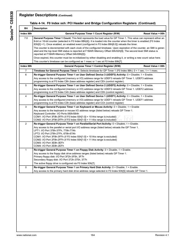 164
164
 165
165
 166
166
 167
167
 168
168
 169
169
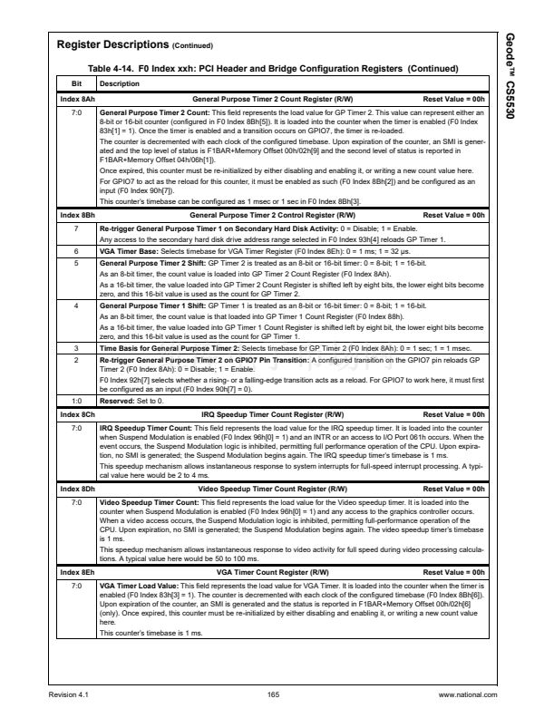
 170
170
 171
171
 172
172
 173
173
 174
174
 175
175
 176
176
 177
177
 178
178
 179
179
 180
180
 181
181
 182
182
 183
183
 184
184
 185
185
 186
186
 187
187
 188
188
 189
189
 190
190
 191
191
 192
192
 193
193
 194
194
 195
195
 196
196
 197
197
 198
198
 199
199
 200
200
 201
201
 202
202
 203
203
 204
204
 205
205
 206
206
 207
207
 208
208
 209
209
 210
210
 211
211
 212
212
 213
213
 214
214
 215
215
 216
216
 217
217
 218
218
 219
219
 220
220
 221
221
 222
222
 223
223
 224
224
 225
225
 226
226
 227
227
 228
228
 229
229
 230
230
 231
231
 232
232
 233
233
 234
234
 235
235
 236
236
 237
237
 238
238
 239
239
 240
240
 241
241
