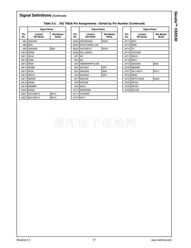
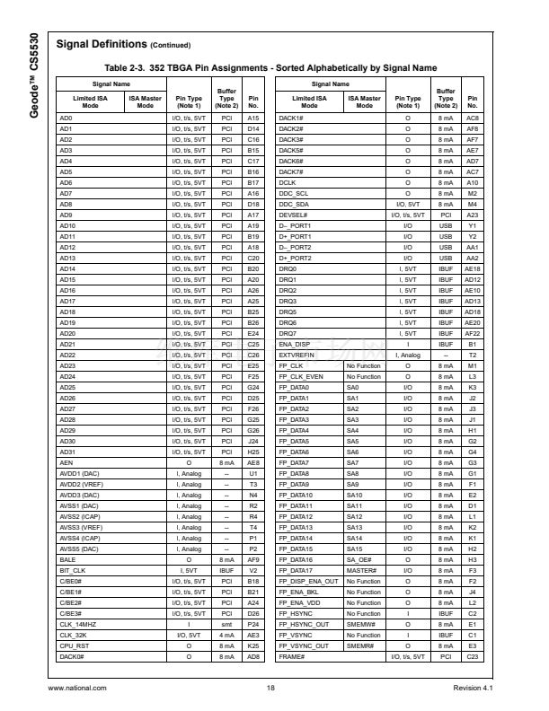
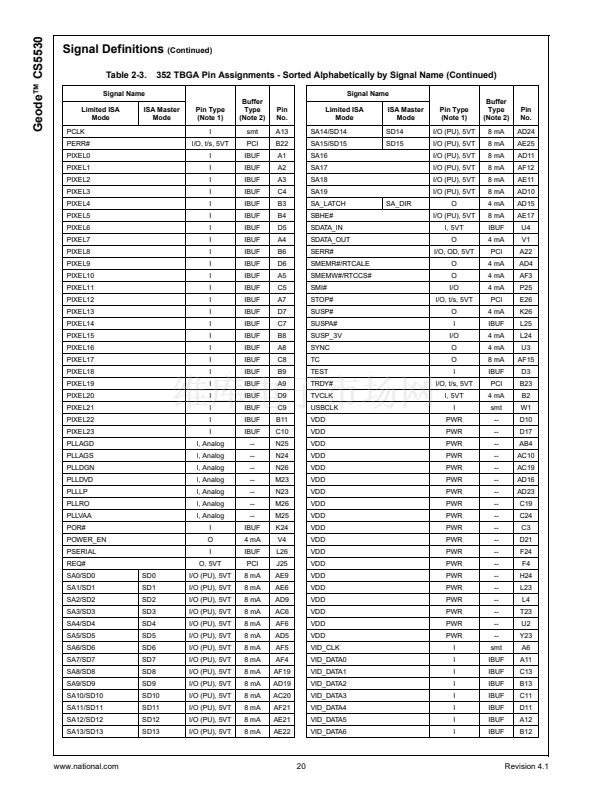
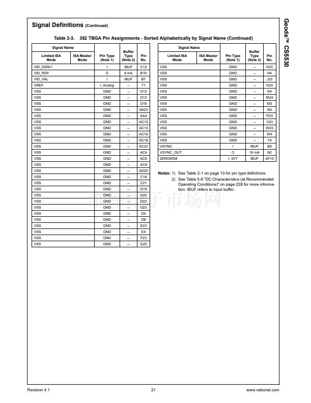
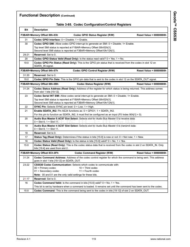
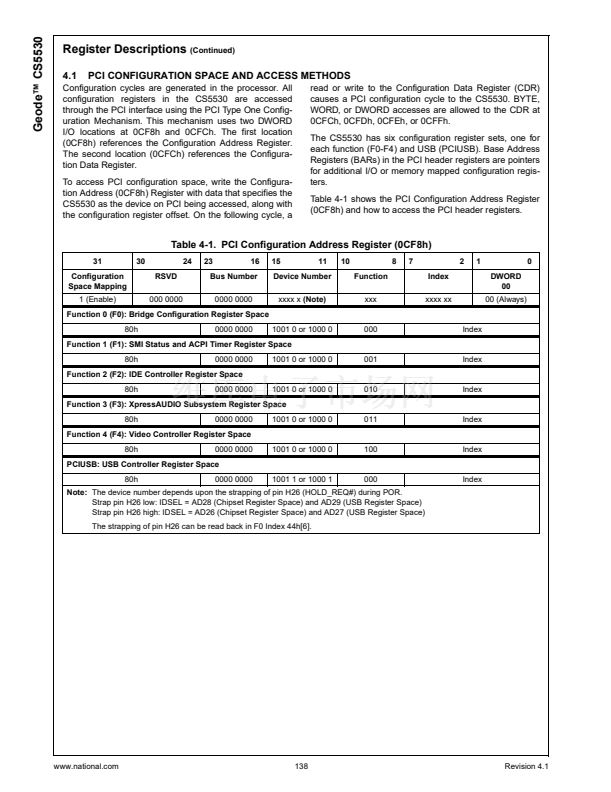
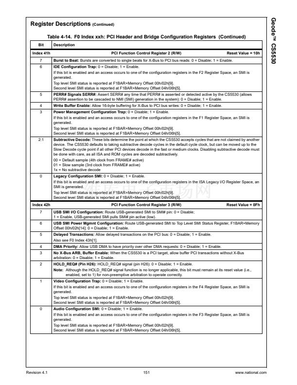
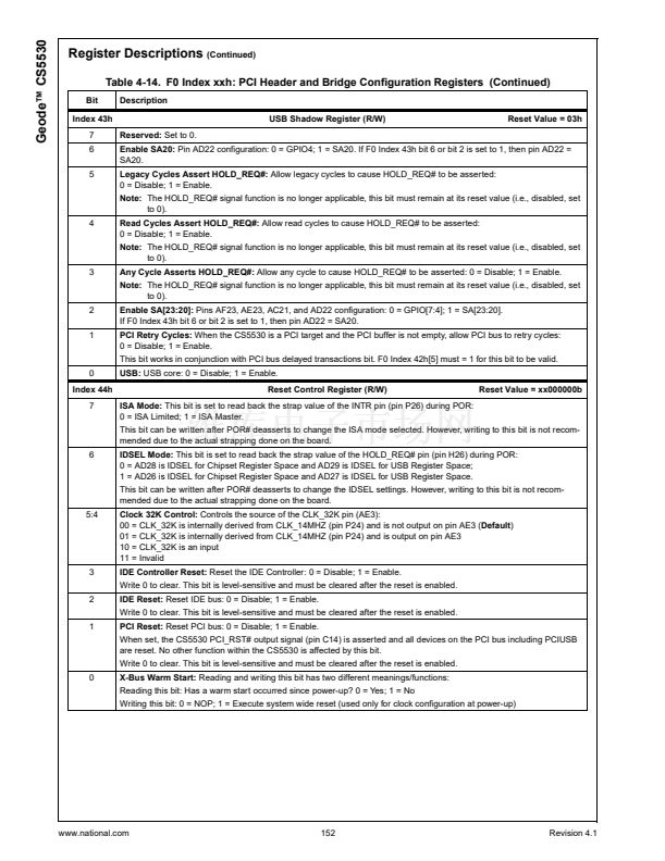
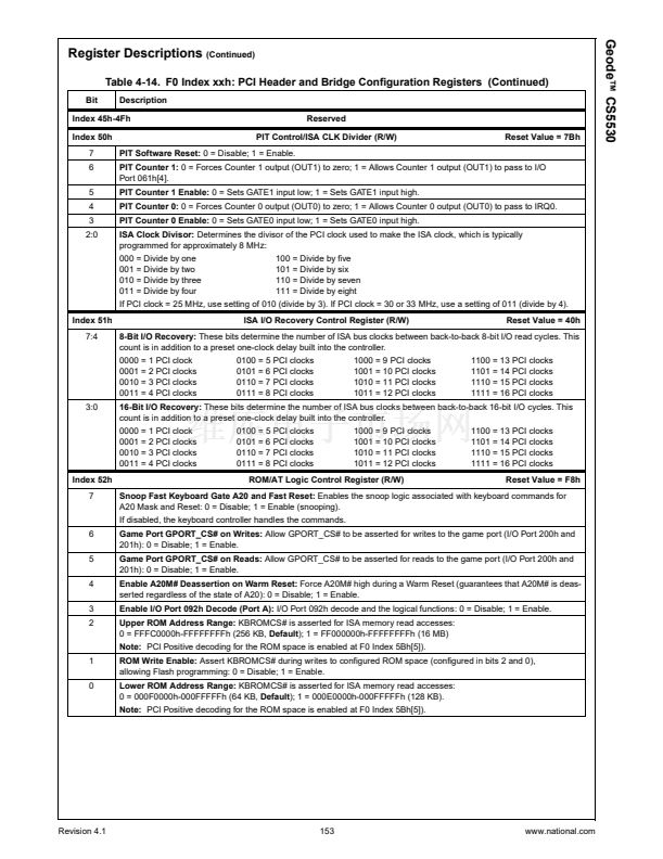
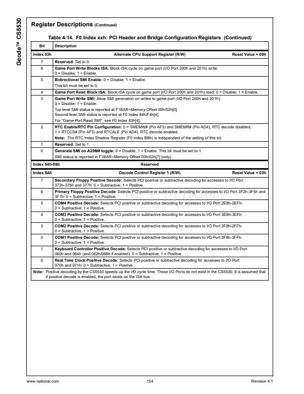
Geode鈩?CS5530
Signal Definitions
(Continued)
2.2.3
CPU Interface (Continued)
Pin
No.
L24
Type
I/O
Description
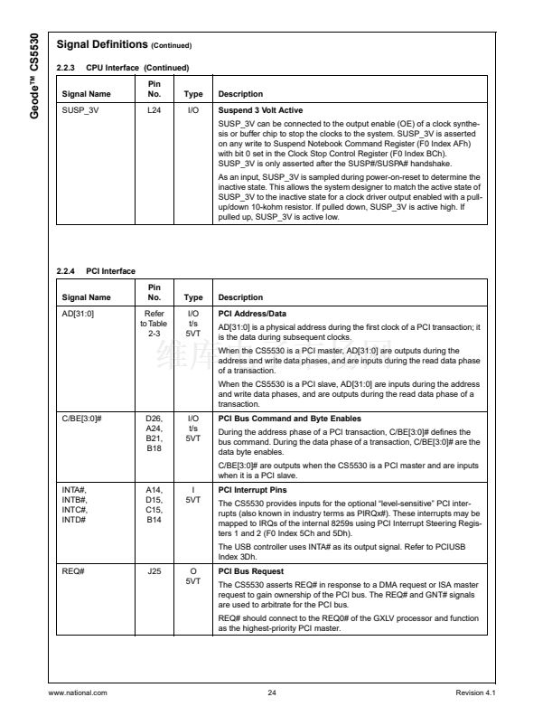
Suspend 3 Volt Active
SUSP_3V can be connected to the output enable (OE) of a clock synthe-
sis or buffer chip to stop the clocks to the system. SUSP_3V is asserted
on any write to Suspend Notebook Command Register (F0 Index AFh)
with bit 0 set in the Clock Stop Control Register (F0 Index BCh).
SUSP_3V is only asserted after the SUSP#/SUSPA# handshake.
As an input, SUSP_3V is sampled during power-on-reset to determine the
inactive state. This allows the system designer to match the active state of
SUSP_3V to the inactive state for a clock driver output enabled with a pull-
up/down 10-kohm resistor. If pulled down, SUSP_3V is active high. If
pulled up, SUSP_3V is active low.
Signal Name
SUSP_3V
2.2.4
PCI Interface
Pin
No.
Refer
to Table
2-3
Type
I/O
t/s
5VT
Description
PCI Address/Data
AD[31:0] is a physical address during the first clock of a PCI transaction; it
is the data during subsequent clocks.
When the CS5530 is a PCI master, AD[31:0] are outputs during the
address and write data phases, and are inputs during the read data phase
of a transaction.
When the CS5530 is a PCI slave, AD[31:0] are inputs during the address
and write data phases, and are outputs during the read data phase of a
transaction.
Signal Name
AD[31:0]
C/BE[3:0]#
D26,
A24,
B21,
B18
I/O
t/s
5VT
PCI Bus Command and Byte Enables
During the address phase of a PCI transaction, C/BE[3:0]# defines the
bus command. During the data phase of a transaction, C/BE[3:0]# are the
data byte enables.
C/BE[3:0]# are outputs when the CS5530 is a PCI master and are inputs
when it is a PCI slave.
INTA#,
INTB#,
INTC#,
INTD#
A14,
D15,
C15,
B14
I
5VT
PCI Interrupt Pins
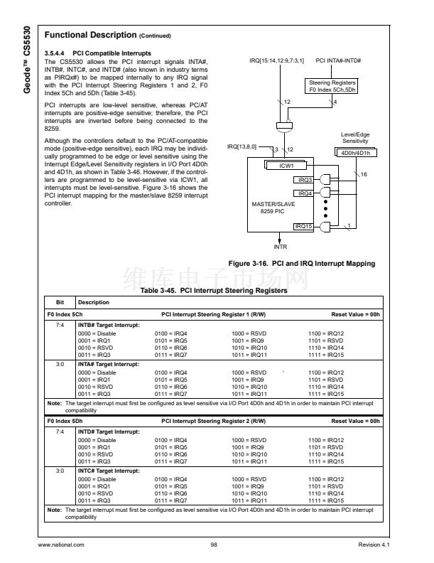
The CS5530 provides inputs for the optional 鈥渓evel-sensitive鈥?PCI inter-
rupts (also known in industry terms as PIRQx#). These interrupts may be
mapped to IRQs of the internal 8259s using PCI Interrupt Steering Regis-
ters 1 and 2 (F0 Index 5Ch and 5Dh).
The USB controller uses INTA# as its output signal. Refer to PCIUSB
Index 3Dh.
REQ#
J25
O
5VT
PCI Bus Request
The CS5530 asserts REQ# in response to a DMA request or ISA master
request to gain ownership of the PCI bus. The REQ# and GNT# signals
are used to arbitrate for the PCI bus.
REQ# should connect to the REQ0# of the GXLV processor and function
as the highest-priority PCI master.
www.national.com
24
Revision 4.1


 1
1
 2
2
 3
3
 4
4
 5
5
 6
6
 7
7
 8
8
 9
9
 10
10
 11
11
 12
12
 13
13
 14
14
 15
15
 16
16
 17
17
 18
18
 19
19
 20
20
 21
21
 22
22
 23
23
 24
24
 25
25
 26
26
 27
27
 28
28
 29
29
 30
30
 31
31
 32
32
 33
33
 34
34
 35
35
 36
36
 37
37
 38
38
 39
39
 40
40
 41
41
 42
42
 43
43
 44
44
 45
45
 46
46
 47
47
 48
48
 49
49
 50
50
 51
51
 52
52
 53
53
 54
54
 55
55
 56
56
 57
57
 58
58
 59
59
 60
60
 61
61
 62
62
 63
63
 64
64
 65
65
 66
66
 67
67
 68
68
 69
69
 70
70
 71
71
 72
72
 73
73
 74
74
 75
75
 76
76
 77
77
 78
78
 79
79
 80
80
 81
81
 82
82
 83
83
 84
84
 85
85
 86
86
 87
87
 88
88
 89
89
 90
90
 91
91
 92
92
 93
93
 94
94
 95
95
 96
96
 97
97
 98
98
 99
99
 100
100
 101
101
 102
102
 103
103
 104
104
 105
105
 106
106
 107
107
 108
108
 109
109
 110
110
 111
111
 112
112
 113
113
 114
114
 115
115
 116
116
 117
117
 118
118
 119
119
 120
120
 121
121
 122
122
 123
123
 124
124
 125
125
 126
126
 127
127
 128
128
 129
129
 130
130
 131
131
 132
132
 133
133
 134
134
 135
135
 136
136
 137
137
 138
138
 139
139
 140
140
 141
141
 142
142
 143
143
 144
144
 145
145
 146
146
 147
147
 148
148
 149
149
 150
150
 151
151
 152
152
 153
153
 154
154
 155
155
 156
156
 157
157
 158
158
 159
159
 160
160
 161
161
 162
162
 163
163
 164
164
 165
165
 166
166
 167
167
 168
168
 169
169
 170
170
 171
171
 172
172
 173
173
 174
174
 175
175
 176
176
 177
177
 178
178
 179
179
 180
180
 181
181
 182
182
 183
183
 184
184
 185
185
 186
186
 187
187
 188
188
 189
189
 190
190
 191
191
 192
192
 193
193
 194
194
 195
195
 196
196
 197
197
 198
198
 199
199
 200
200
 201
201
 202
202
 203
203
 204
204
 205
205
 206
206
 207
207
 208
208
 209
209
 210
210
 211
211
 212
212
 213
213
 214
214
 215
215
 216
216
 217
217
 218
218
 219
219
 220
220
 221
221
 222
222
 223
223
 224
224
 225
225
 226
226
 227
227
 228
228
 229
229
 230
230
 231
231
 232
232
 233
233
 234
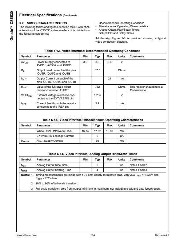
234
 235
235
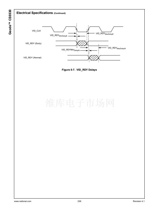 236
236
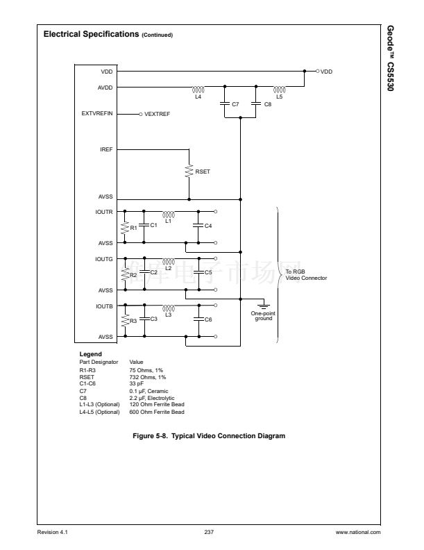 237
237
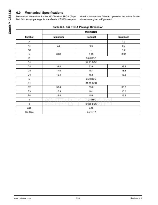 238
238
 239
239
 240
240
 241
241
