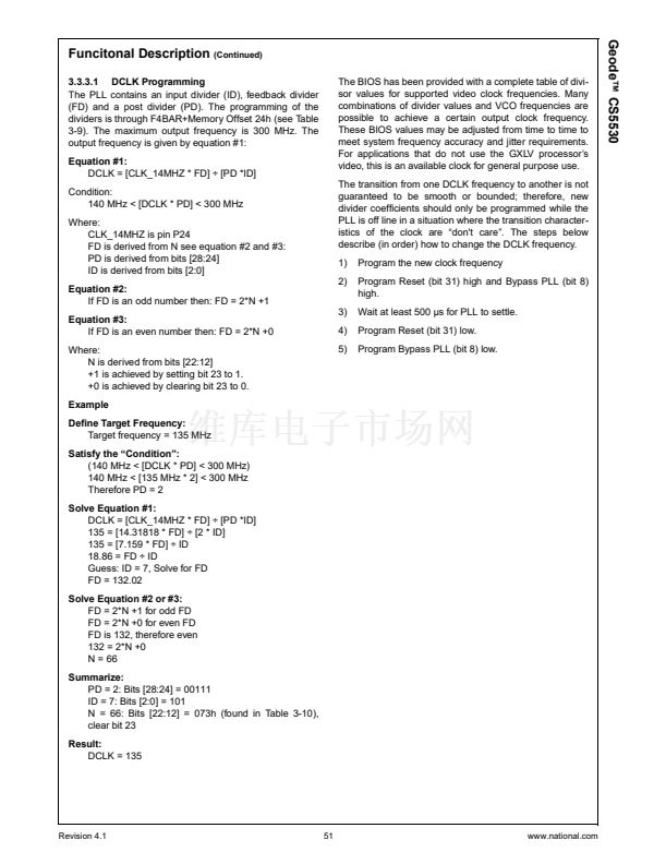
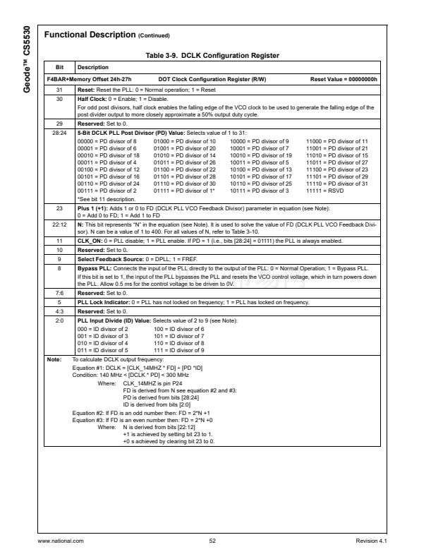
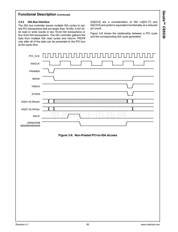
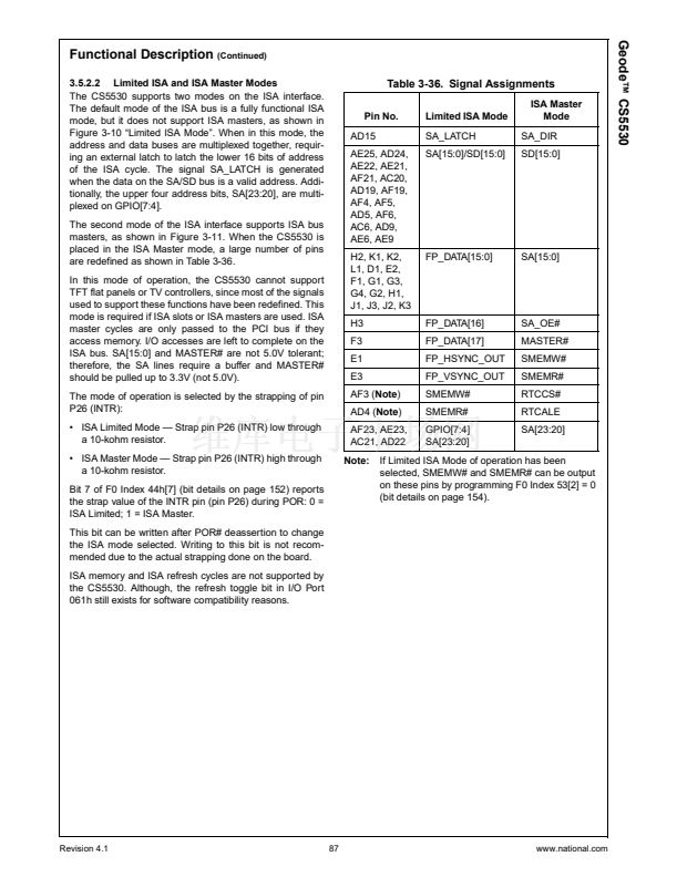
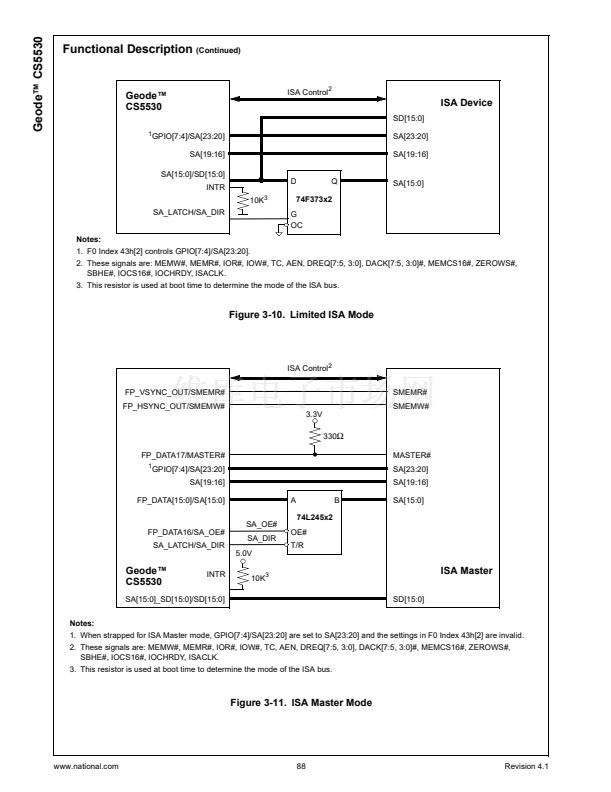
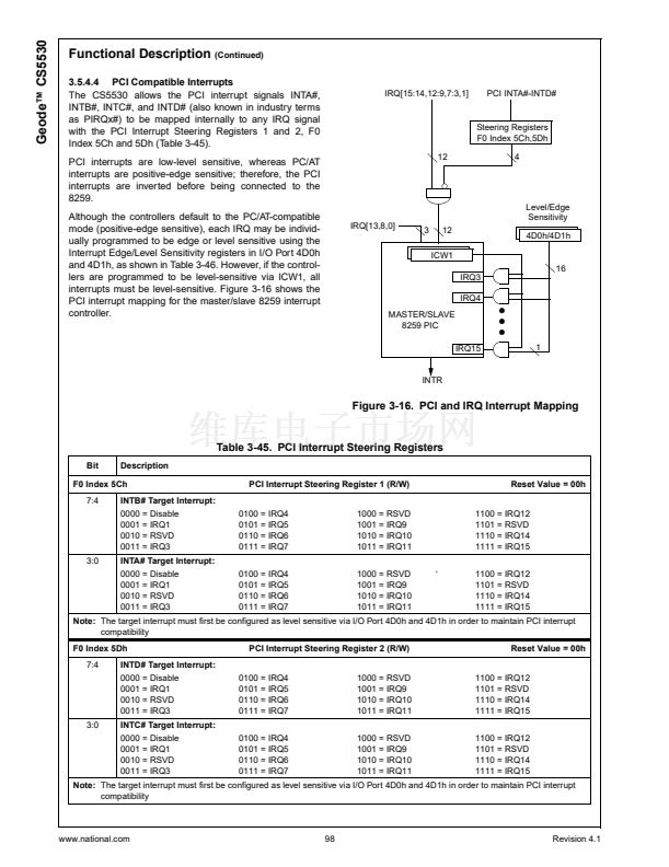
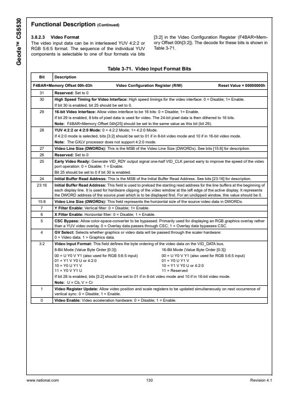
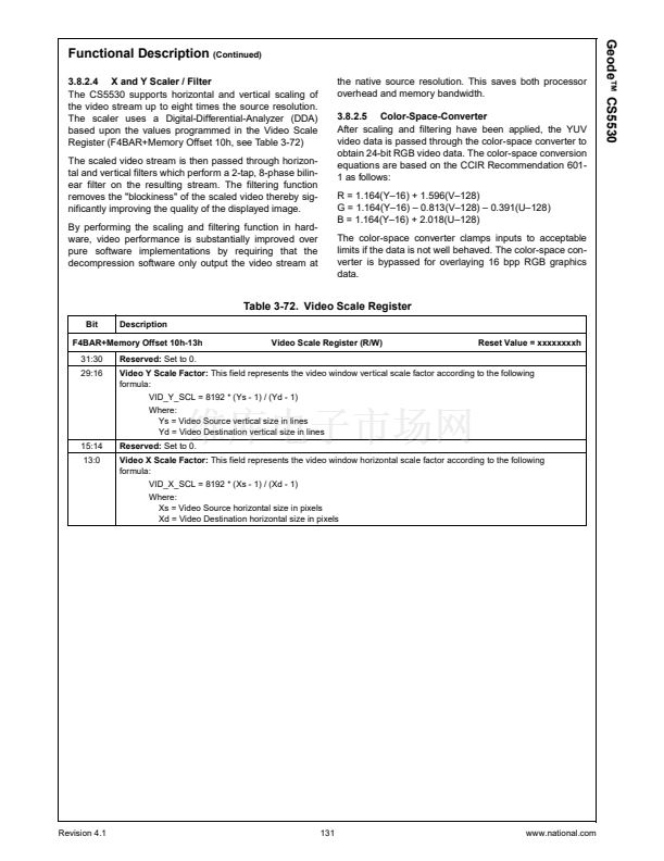
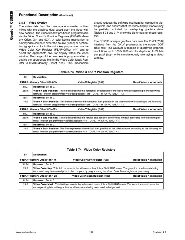
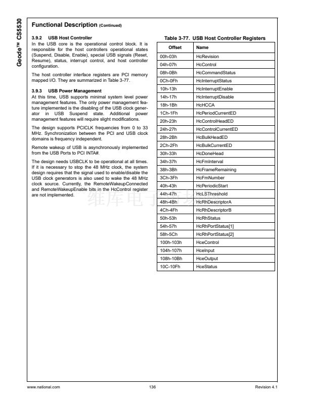
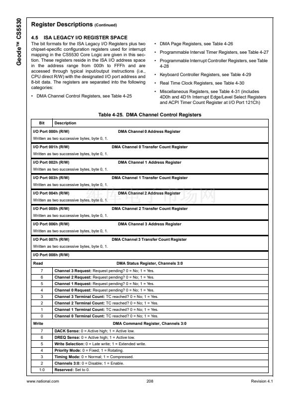
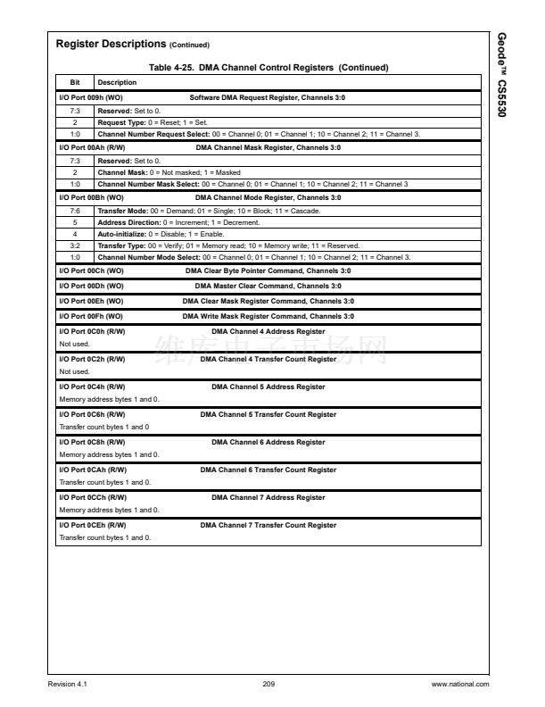
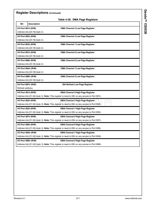
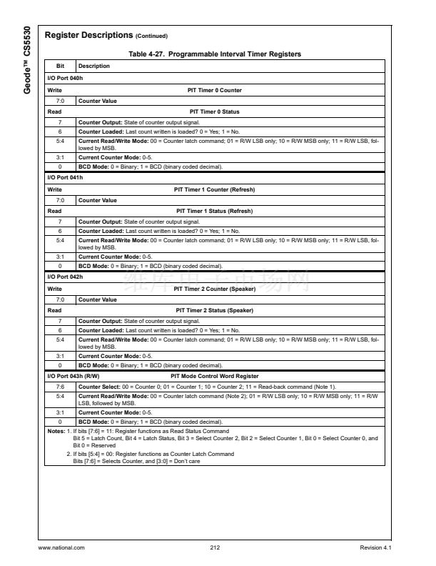
Geode鈩?CS5530
Functional Description
(Continued)
3.4
POWER MANAGEMENT
address register in Function 1 (F1) at Index 10h (F1BAR).
F1BAR sets the base address for the SMI status and
ACPI timer support registers as shown in Table 3-11.
3.4.1 APM Support
Many notebook computers rely solely on an APM
(Advanced Power Management) driver for enabling the
operating system to power-manage the CPU. APM pro-
vides several services which enhance the system power
management and is theoretically the best approach; but in
its current form, APM is imperfect for the following rea-
sons:
鈥?APM is an OS-specific driver, and may not be available
for some operating systems.
鈥?Application support is inconsistent. Some applications
in foreground may prevent Idle calls.
鈥?APM does not help with Suspend determination or
peripheral power management.
The CS5530 provides two entry points for APM support:
鈥?Software CPU Suspend control via the CPU Suspend
Command Register (F0 Index AEh)
鈥?Software SMI entry via the Software SMI Register (F0
Index D0h). This allows the APM BIOS to be part of the
SMI handler.
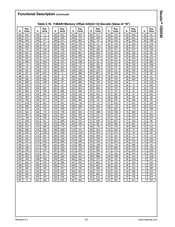
These registers are shown in Table 3-12.
The power management resources provided by a com-
bined CS5530/GXLV processor based system supports a
full-featured notebook implementation. The following
explanations pertain to a full-featured 鈥渘otebook鈥?power
management system. The extent to which these
resources are employed depends on the application and
on the discretion of the system designer.
Power management resources can be grouped according
to the function they enable or support. The major func-
tions are as follows:
鈥?APM Support
鈥?CPU Power Management
- Suspend Modulation
- 3 Volt Suspend
- Save-to-Disk
鈥?Peripheral Power Management
- Device Idle Timers and Traps
- General Purpose Timers
- ACPI Timer Register
- General Purpose I/O Pins
- Power Management SMI Status Reporting Registers
Included in the following subsections are details regarding
the registers used for configuring power management fea-
tures. The majority of these registers are directly
accessed through the PCI configuration register space
designated as Function 0 (F0). However, included in the
discussions are references to F1BAR+Memory Offset
xxh. This refers to the registers accessed through a base
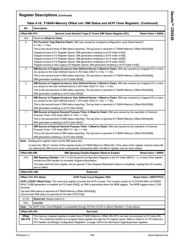
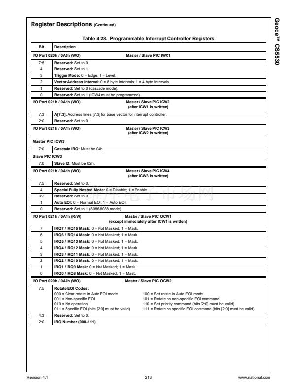
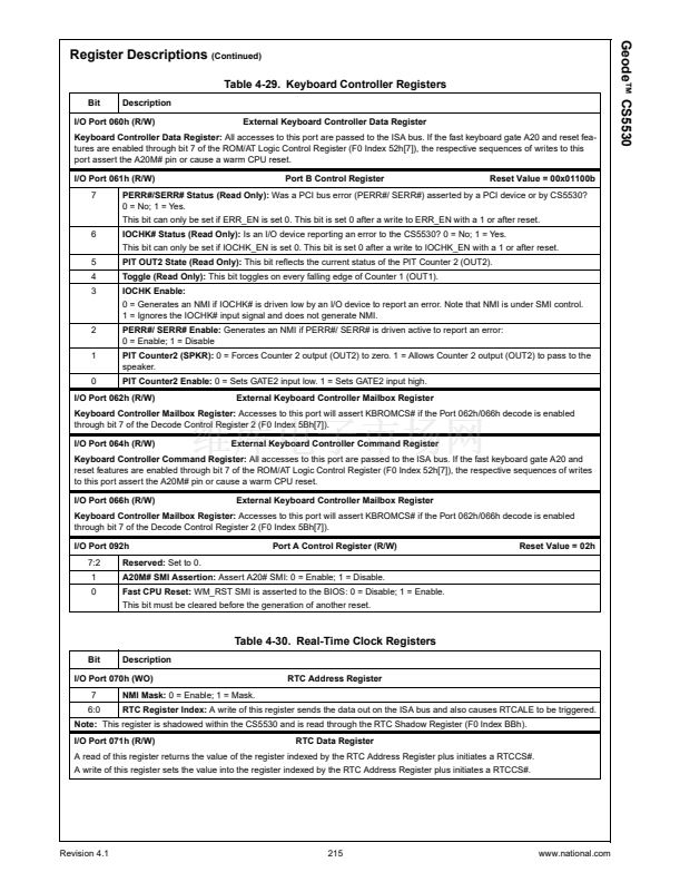
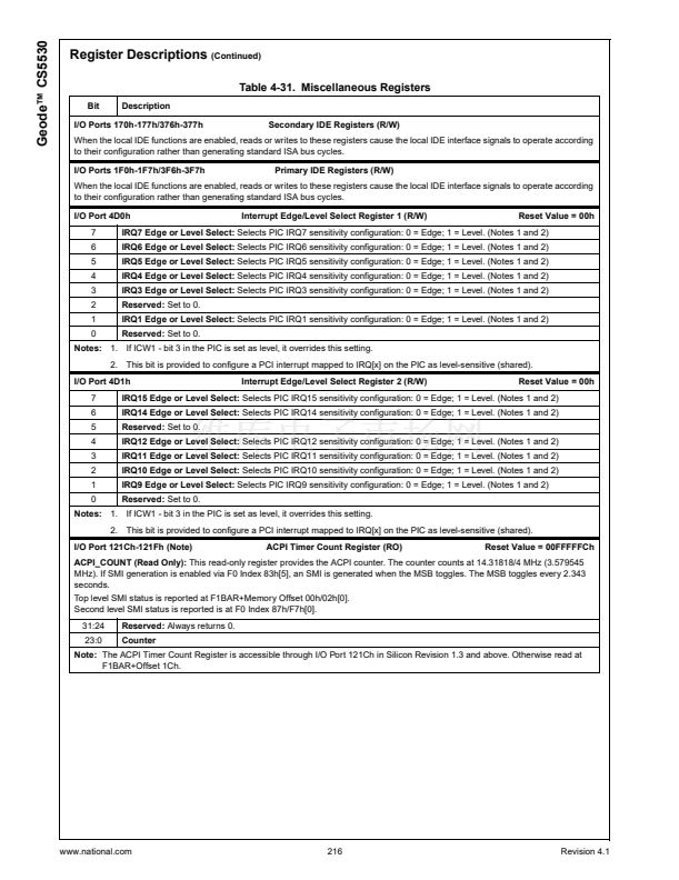
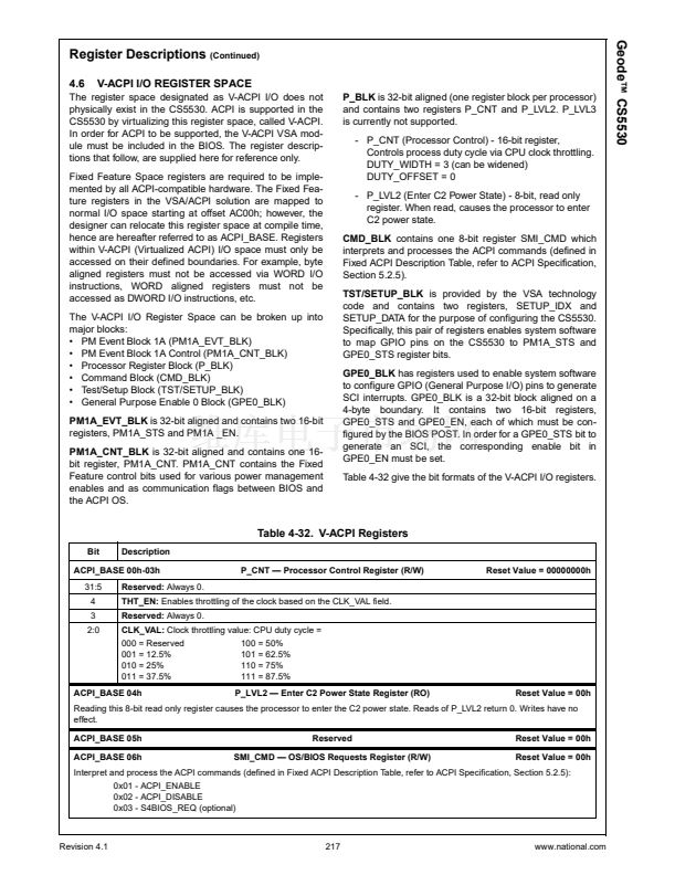
Table 3-11. Base Address Register (F1BAR) for SMI Status and ACPI Timer Support
Bit
Description
Base Address Register - F1BAR (R/W)
Reset Value = 00000000h
F1 Index 10h-13h
This register sets the base address of the memory mapped SMI status and ACPI timer related registers. Bits [7:0] are read only (00h),
indicating a 256 byte memory address range. Refer to Table 4-16 for the SMI status and ACPI timer registers bit formats and reset val-
ues. The upper 16 bytes are always mapped to the ACPI timer, and are always memory mapped.
Note:
In Silicon Revision 1.3 and above the ACPI Timer Count Register is accessible through I/O Port 121Ch.
31:8
7:0
SMI Status/Power Management Base Address
Address Range (Read Only)
www.national.com
54
Revision 4.1


 1
1
 2
2
 3
3
 4
4
 5
5
 6
6
 7
7
 8
8
 9
9
 10
10
 11
11
 12
12
 13
13
 14
14
 15
15
 16
16
 17
17
 18
18
 19
19
 20
20
 21
21
 22
22
 23
23
 24
24
 25
25
 26
26
 27
27
 28
28
 29
29
 30
30
 31
31
 32
32
 33
33
 34
34
 35
35
 36
36
 37
37
 38
38
 39
39
 40
40
 41
41
 42
42
 43
43
 44
44
 45
45
 46
46
 47
47
 48
48
 49
49
 50
50
 51
51
 52
52
 53
53
 54
54
 55
55
 56
56
 57
57
 58
58
 59
59
 60
60
 61
61
 62
62
 63
63
 64
64
 65
65
 66
66
 67
67
 68
68
 69
69
 70
70
 71
71
 72
72
 73
73
 74
74
 75
75
 76
76
 77
77
 78
78
 79
79
 80
80
 81
81
 82
82
 83
83
 84
84
 85
85
 86
86
 87
87
 88
88
 89
89
 90
90
 91
91
 92
92
 93
93
 94
94
 95
95
 96
96
 97
97
 98
98
 99
99
 100
100
 101
101
 102
102
 103
103
 104
104
 105
105
 106
106
 107
107
 108
108
 109
109
 110
110
 111
111
 112
112
 113
113
 114
114
 115
115
 116
116
 117
117
 118
118
 119
119
 120
120
 121
121
 122
122
 123
123
 124
124
 125
125
 126
126
 127
127
 128
128
 129
129
 130
130
 131
131
 132
132
 133
133
 134
134
 135
135
 136
136
 137
137
 138
138
 139
139
 140
140
 141
141
 142
142
 143
143
 144
144
 145
145
 146
146
 147
147
 148
148
 149
149
 150
150
 151
151
 152
152
 153
153
 154
154
 155
155
 156
156
 157
157
 158
158
 159
159
 160
160
 161
161
 162
162
 163
163
 164
164
 165
165
 166
166
 167
167
 168
168
 169
169
 170
170
 171
171
 172
172
 173
173
 174
174
 175
175
 176
176
 177
177
 178
178
 179
179
 180
180
 181
181
 182
182
 183
183
 184
184
 185
185
 186
186
 187
187
 188
188
 189
189
 190
190
 191
191
 192
192
 193
193
 194
194
 195
195
 196
196
 197
197
 198
198
 199
199
 200
200
 201
201
 202
202
 203
203
 204
204
 205
205
 206
206
 207
207
 208
208
 209
209
 210
210
 211
211
 212
212
 213
213
 214
214
 215
215
 216
216
 217
217
 218
218
 219
219
 220
220
 221
221
 222
222
 223
223
 224
224
 225
225
 226
226
 227
227
 228
228
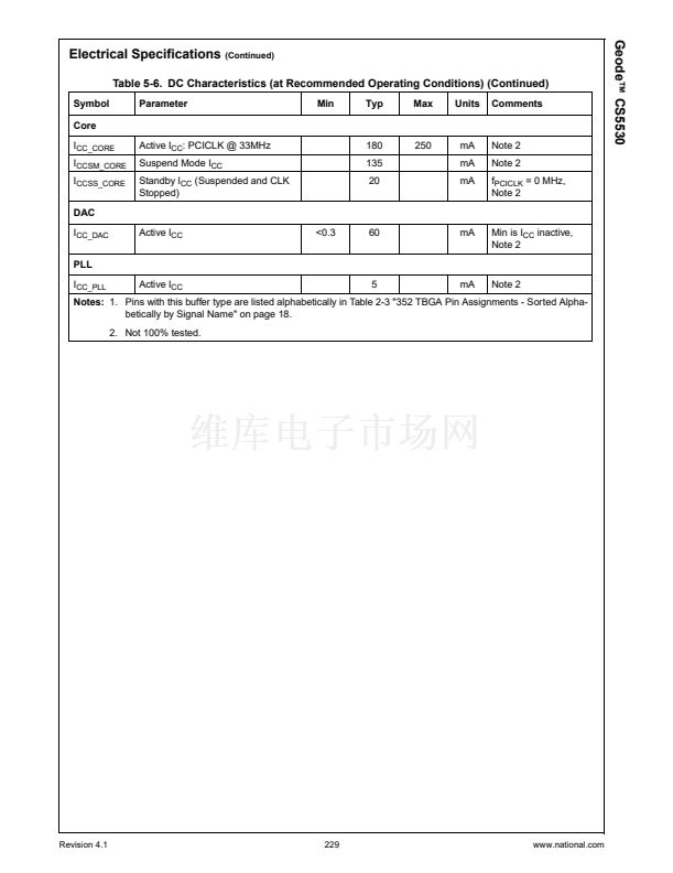 229
229
 230
230
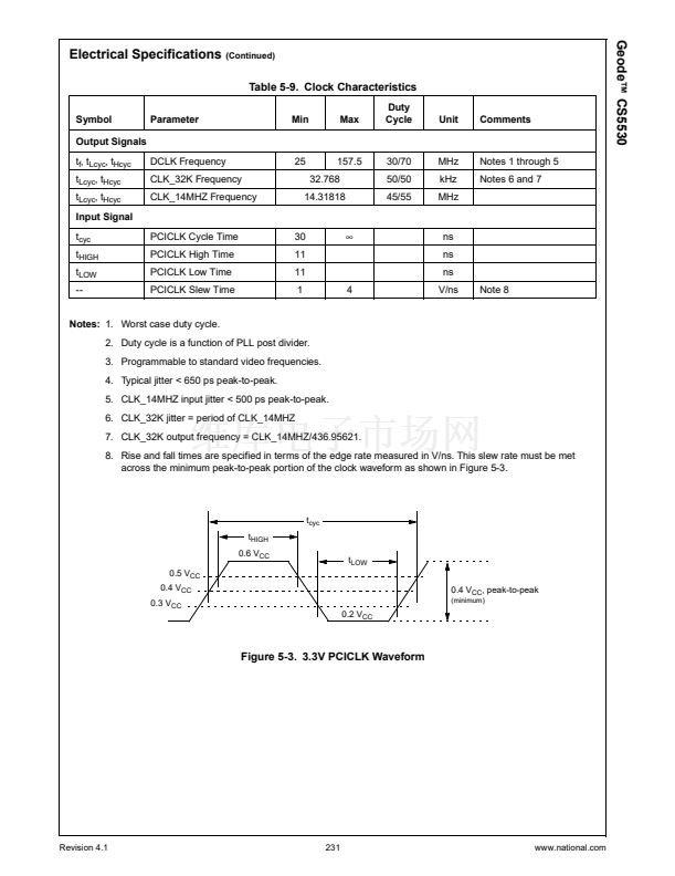 231
231
 232
232
 233
233
 234
234
 235
235
 236
236
 237
237
 238
238
 239
239
 240
240
 241
241
