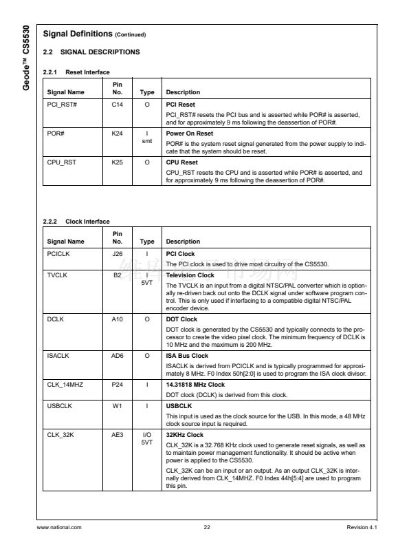
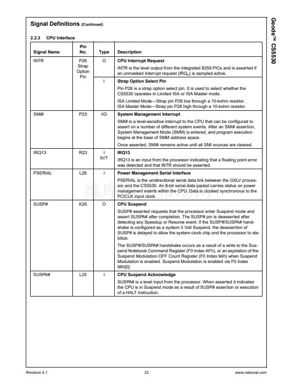
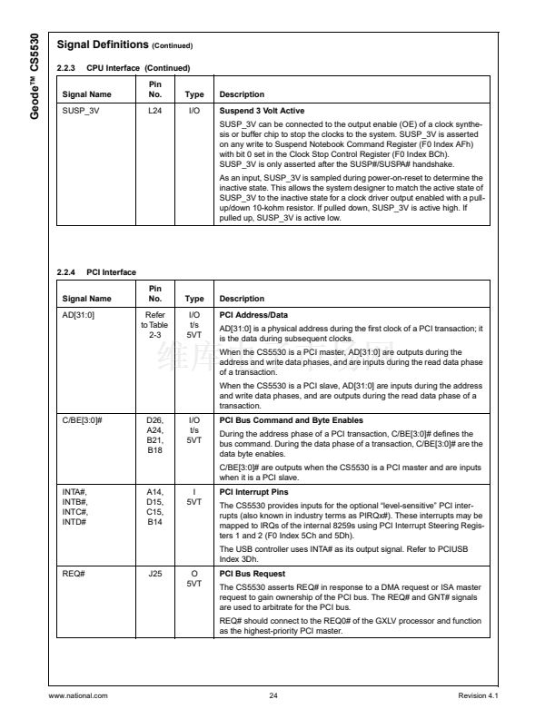
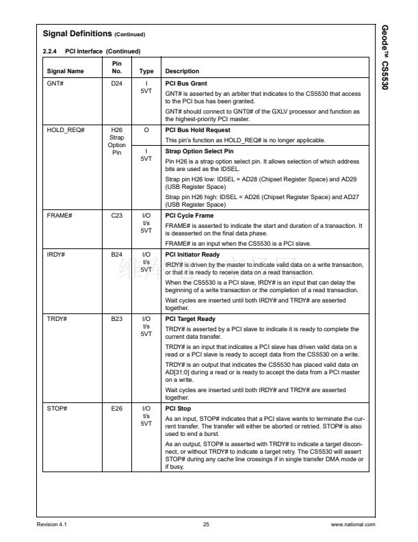
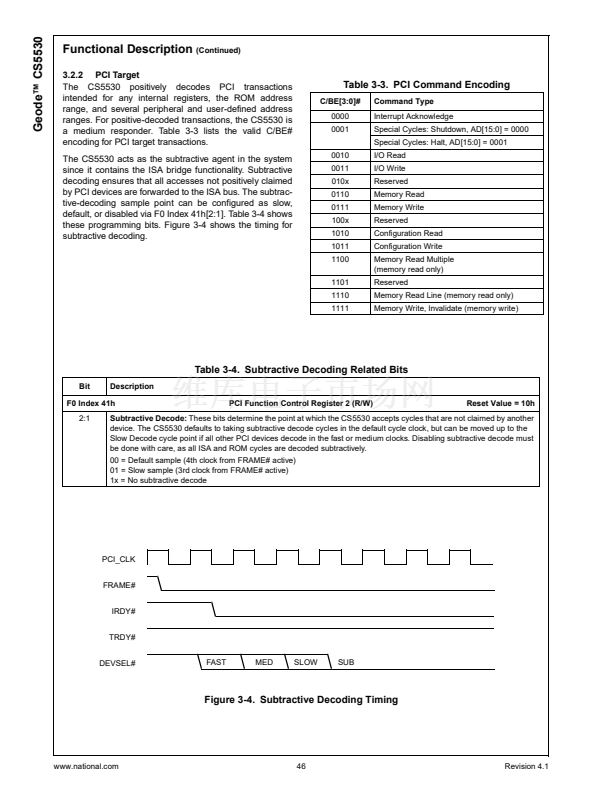
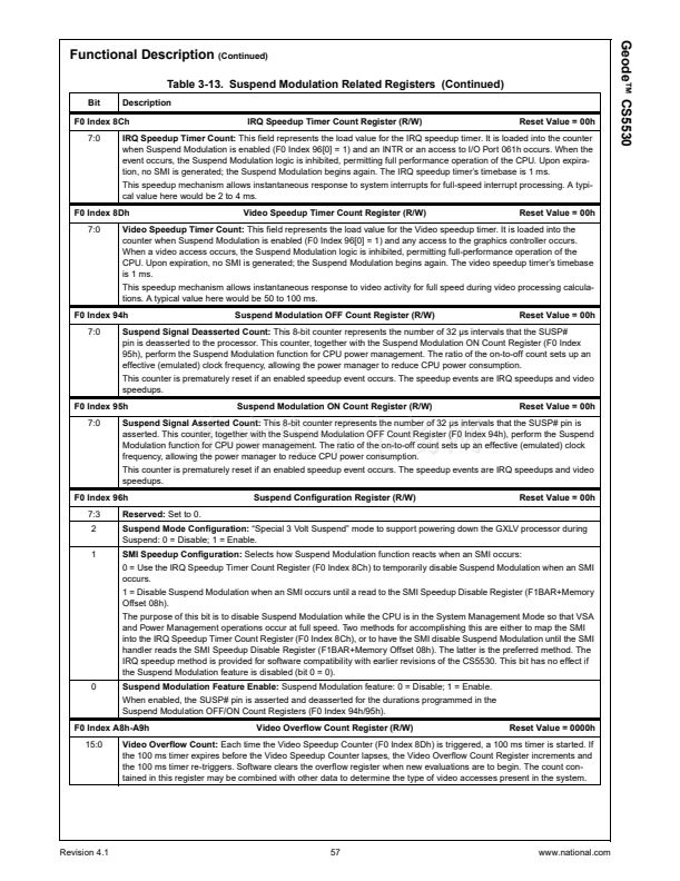
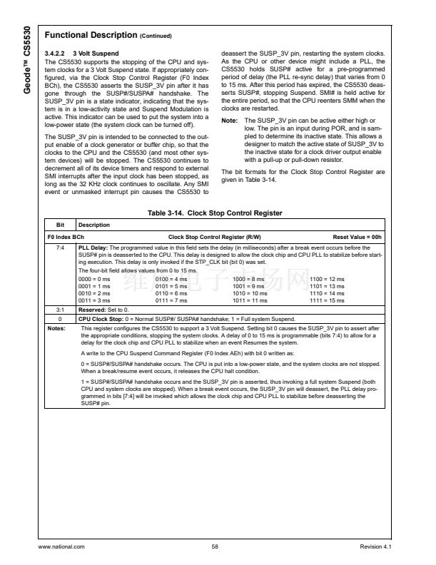
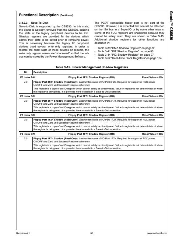
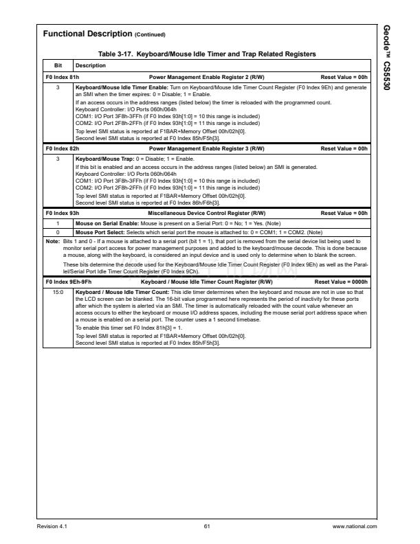
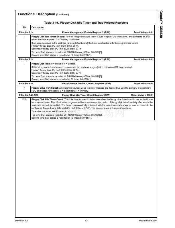
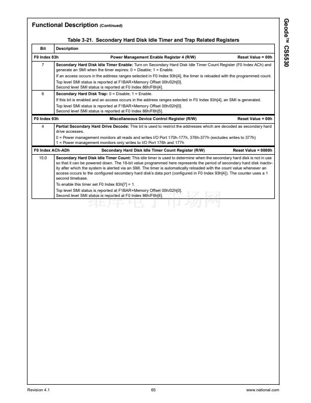
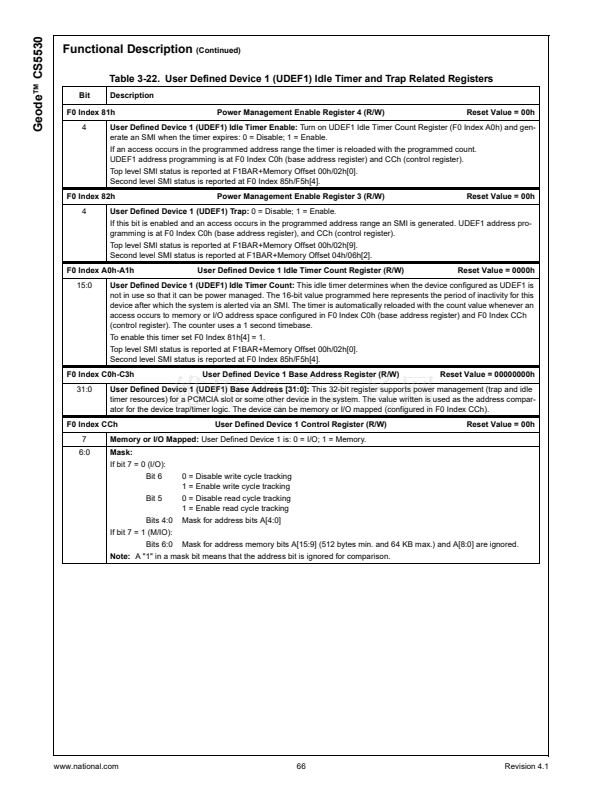
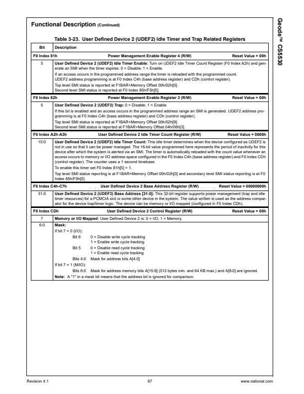
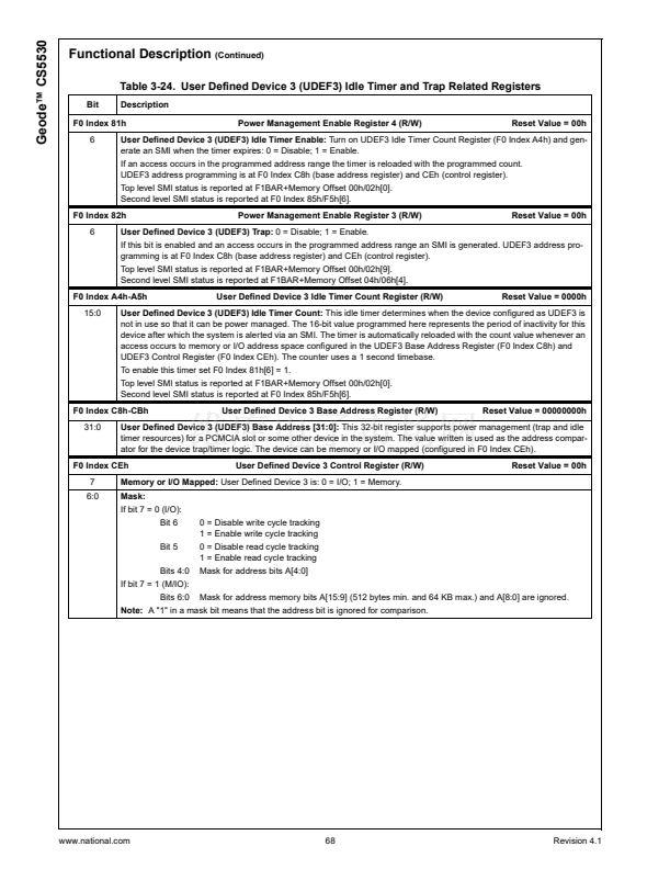
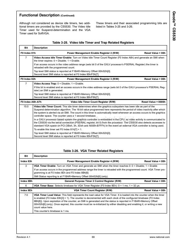
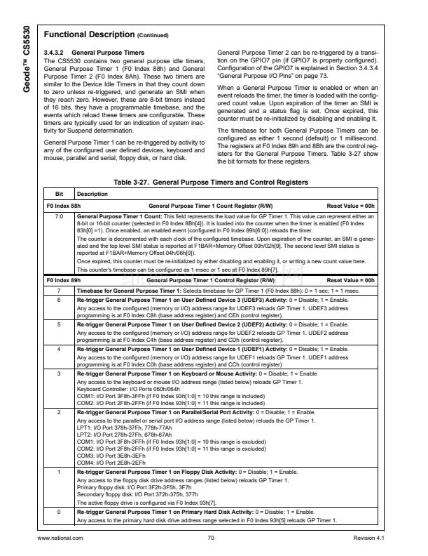
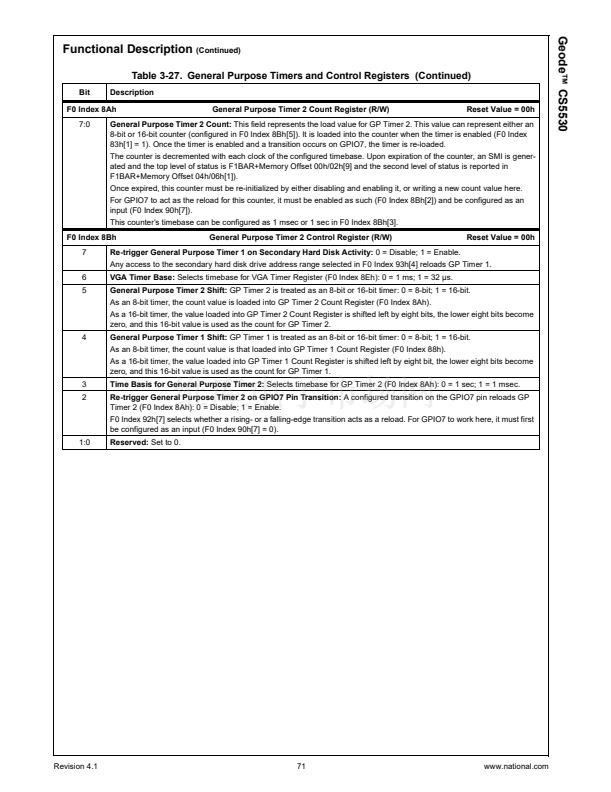
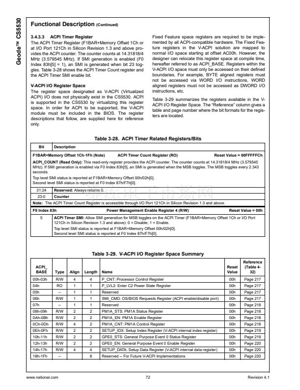
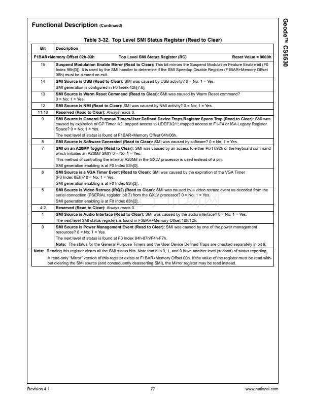
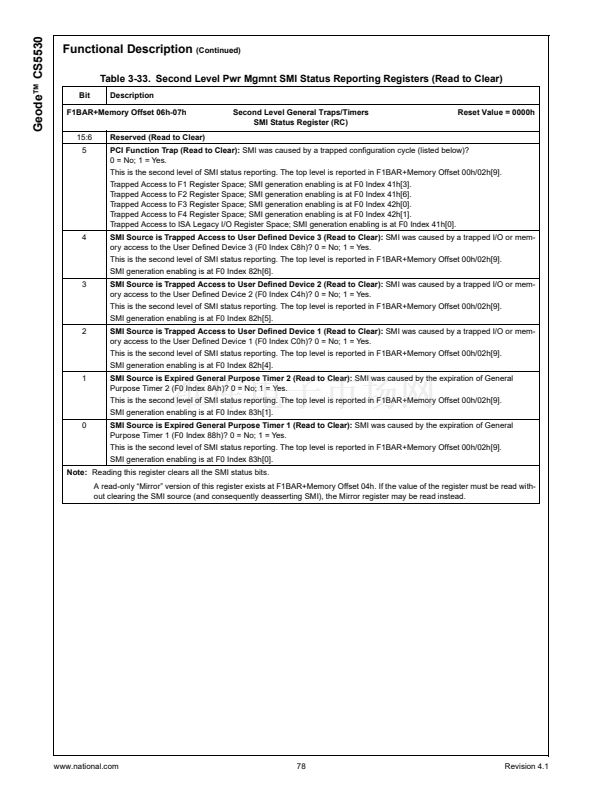
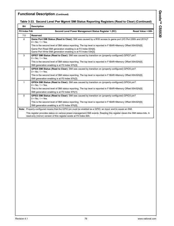
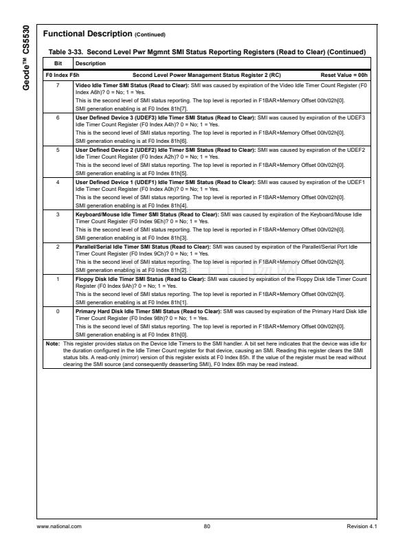
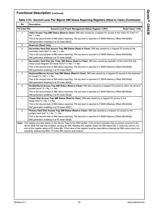
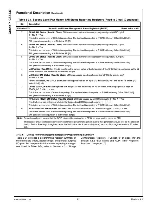
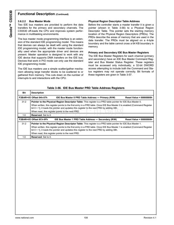
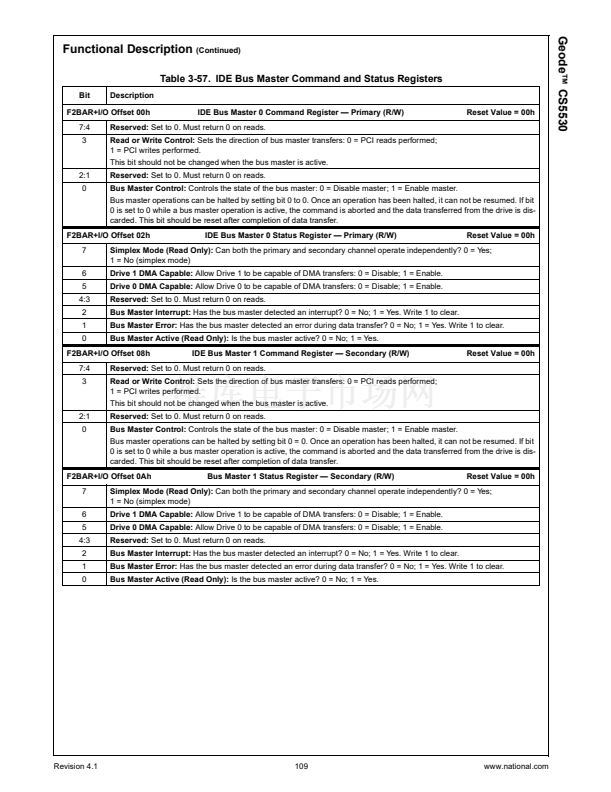
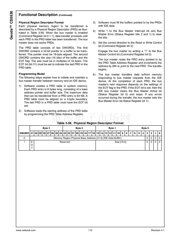
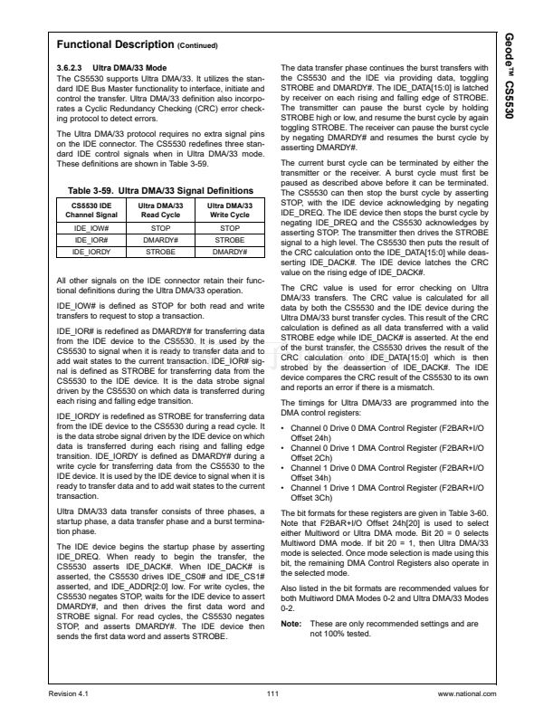
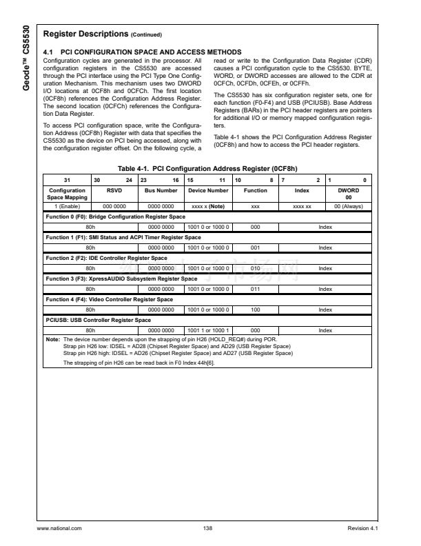
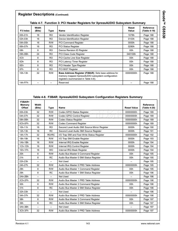
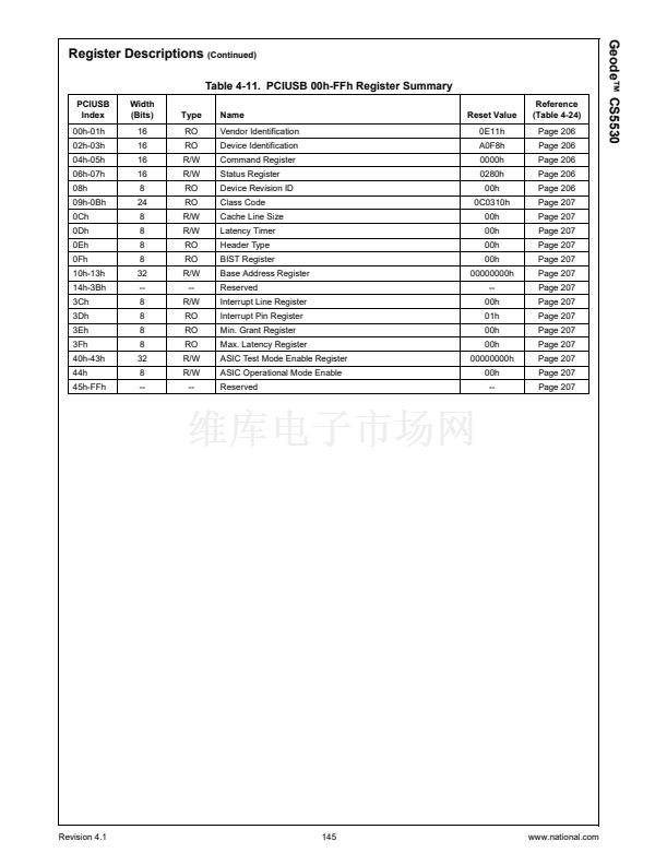
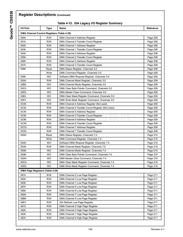
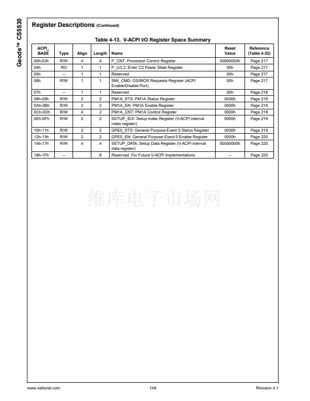
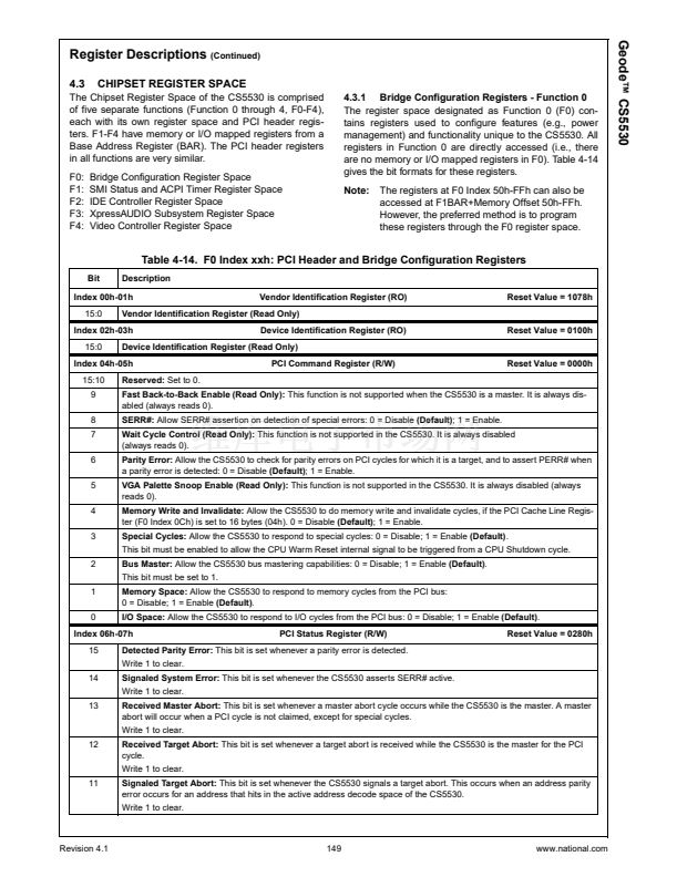
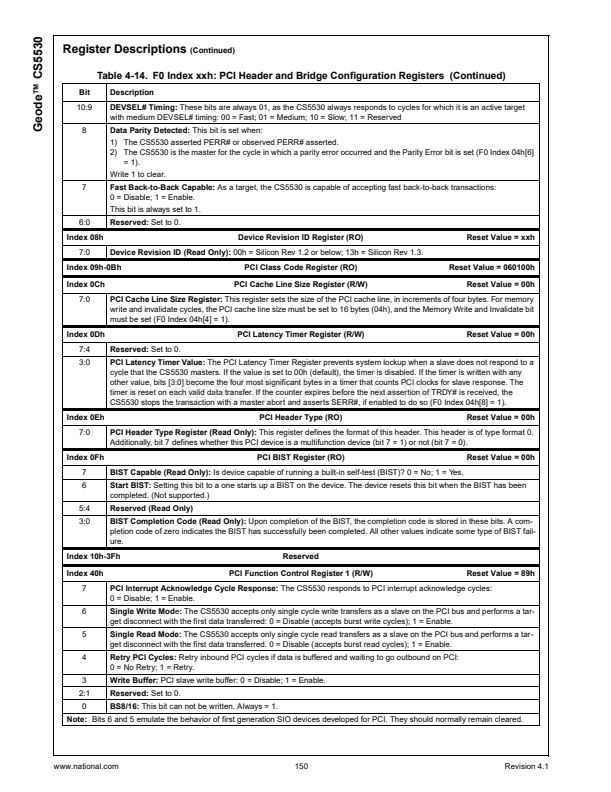
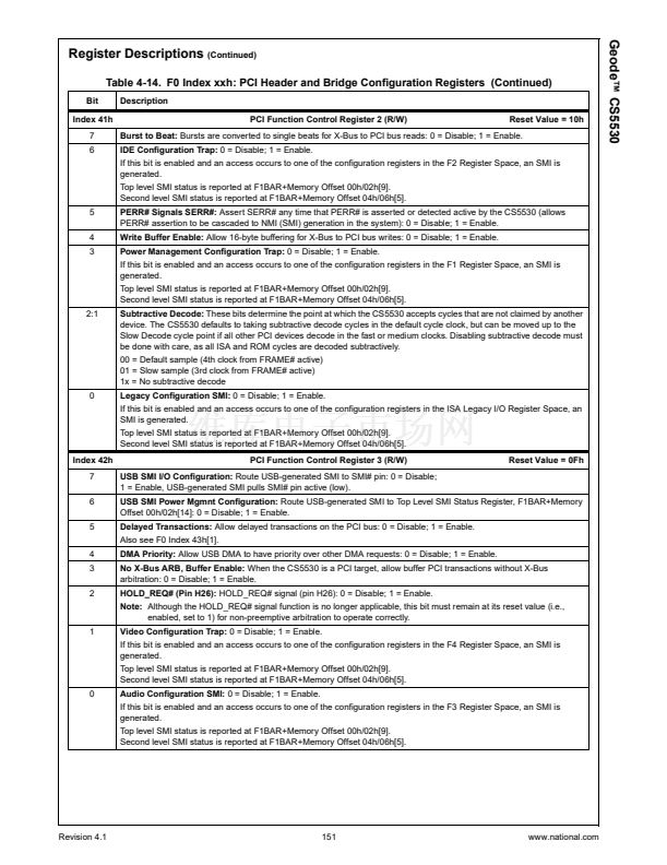
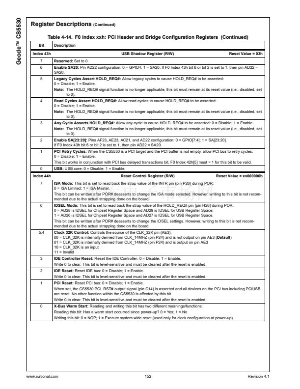
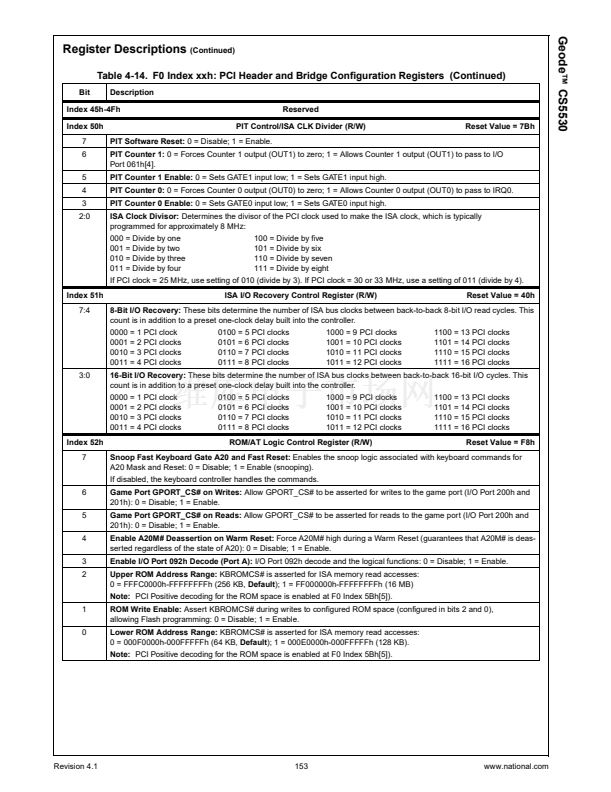
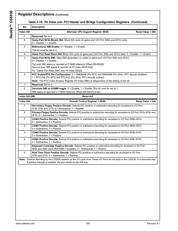
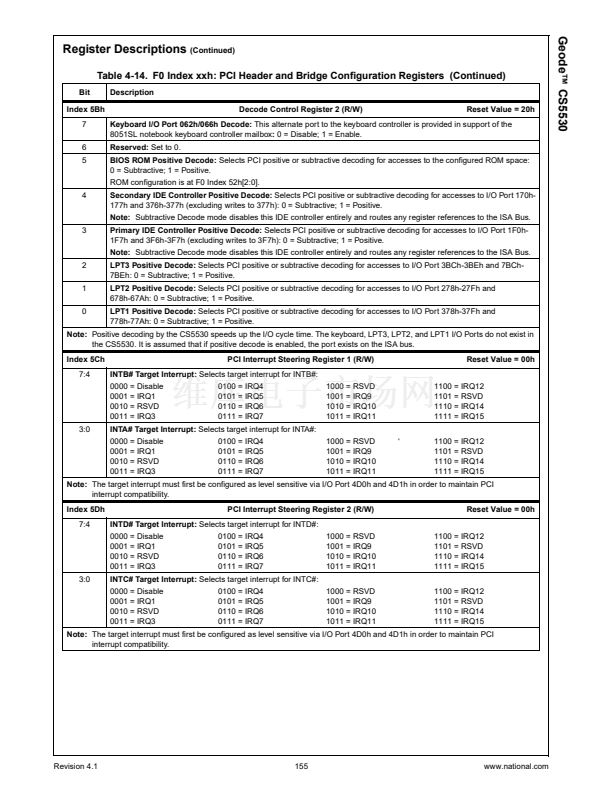
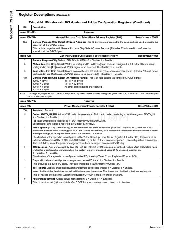
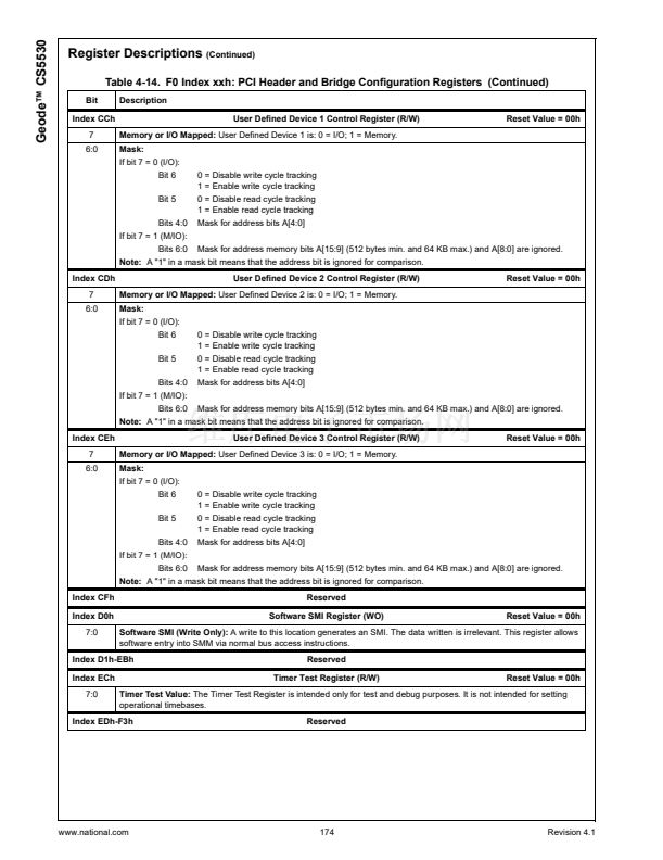
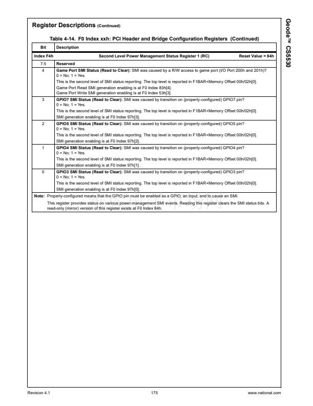
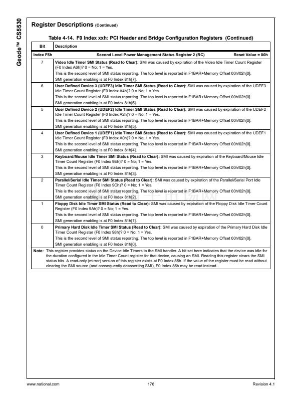
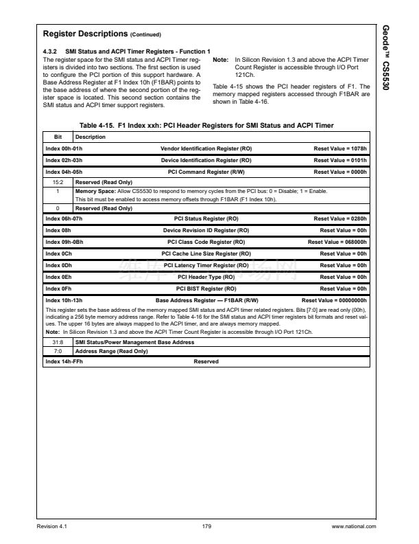
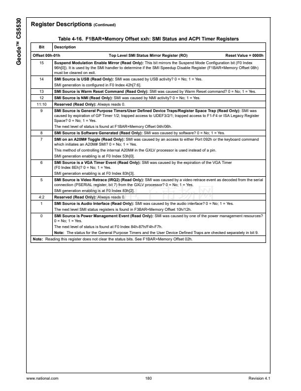
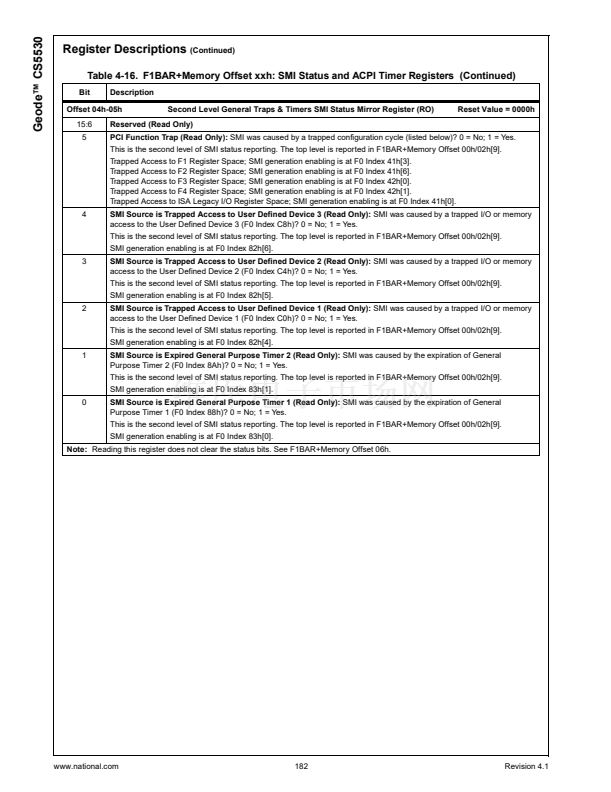
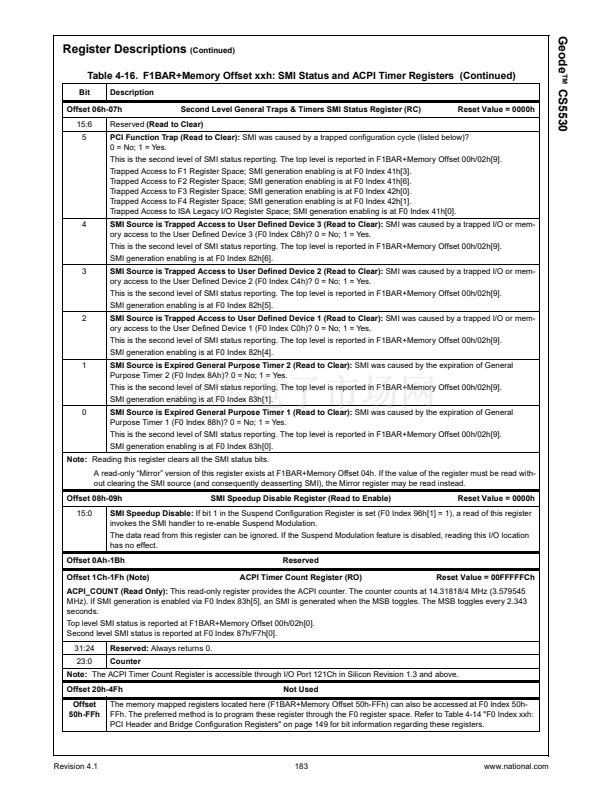
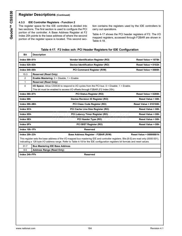
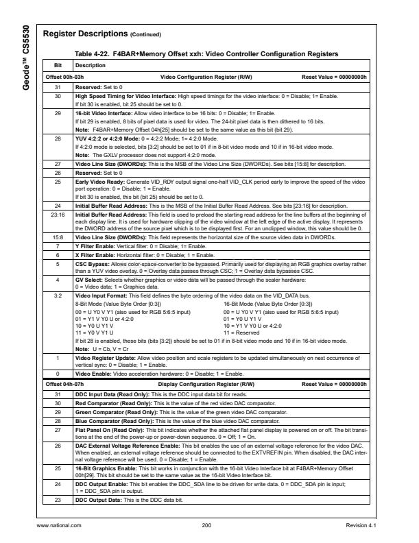
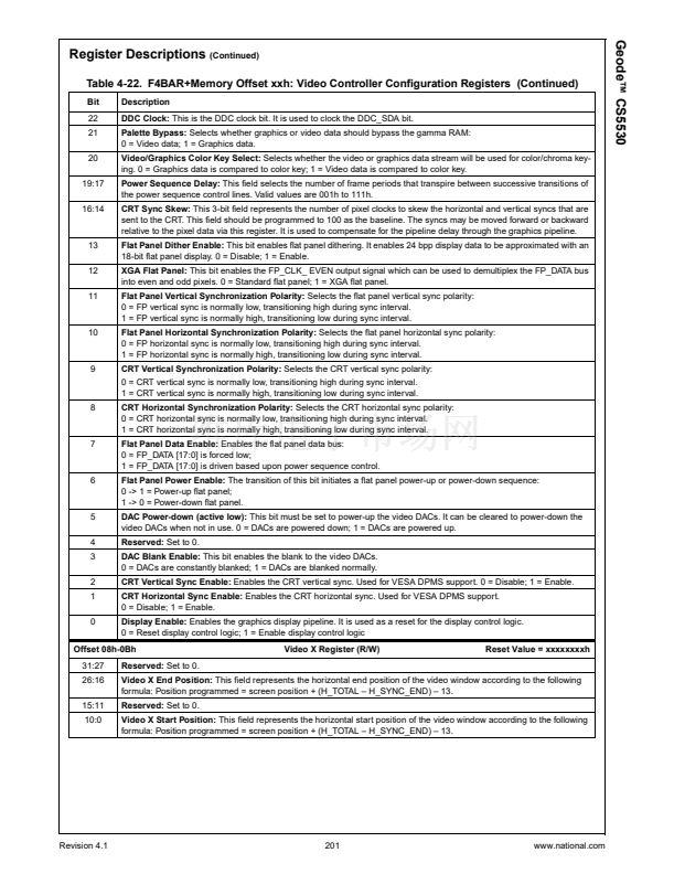
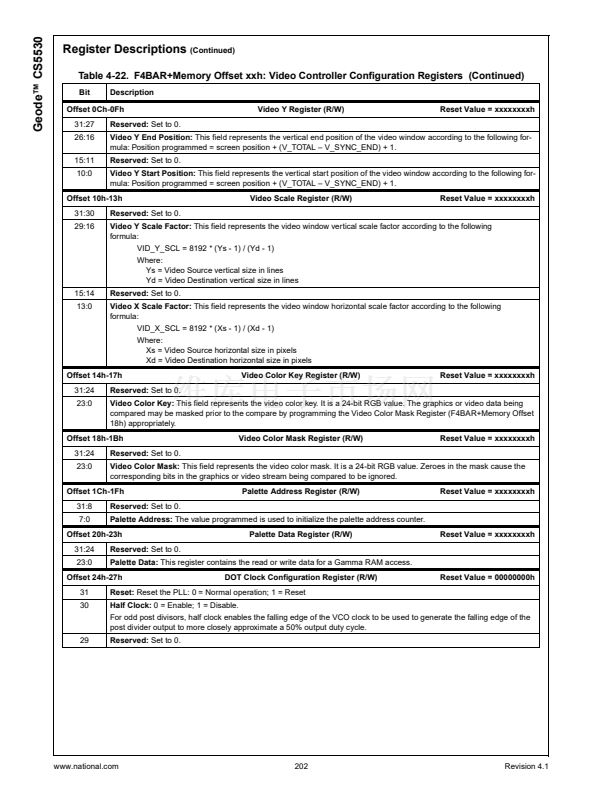
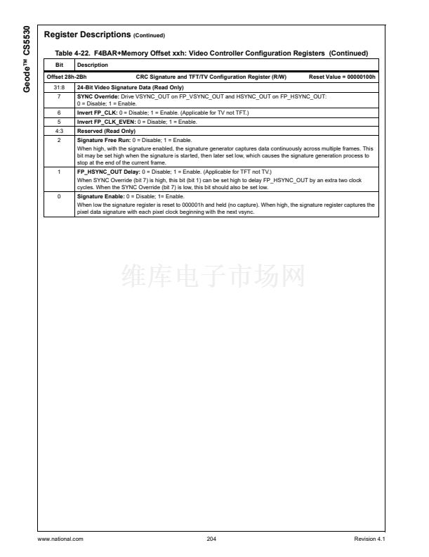
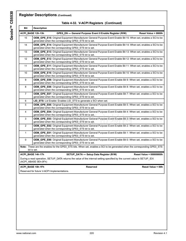
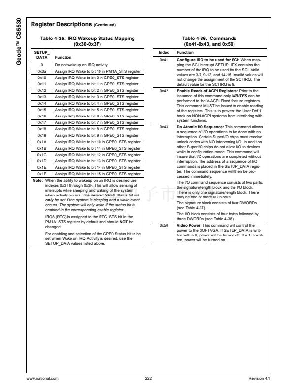
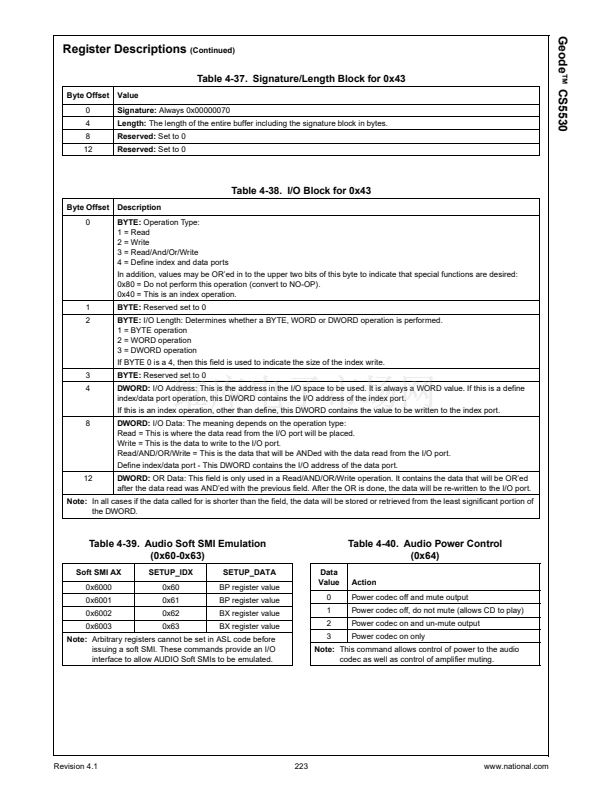
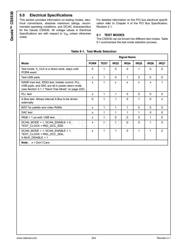
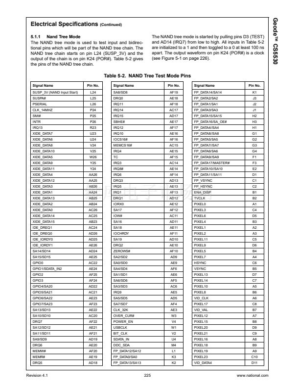
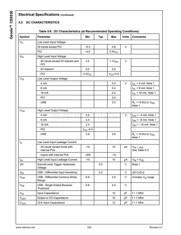
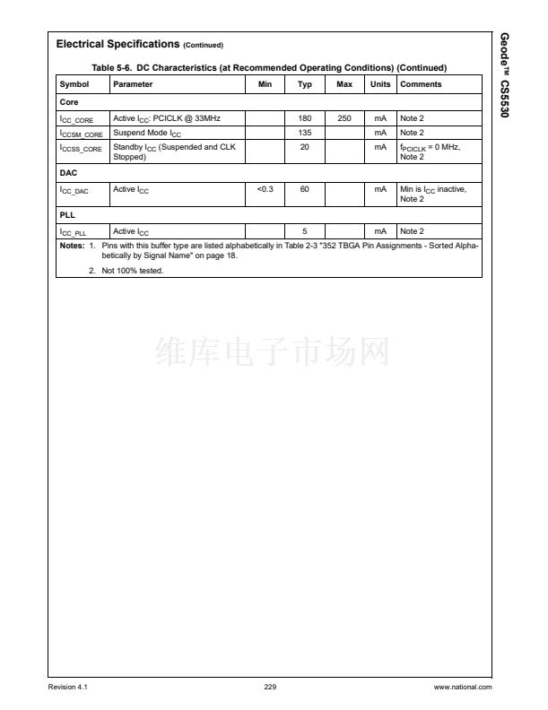
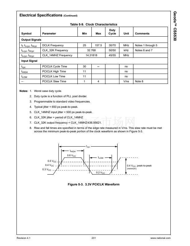
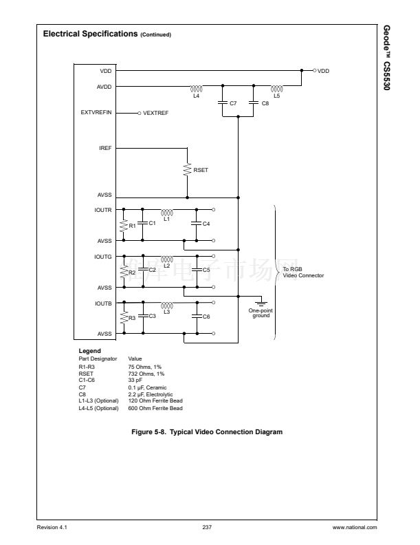
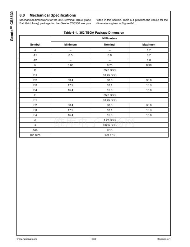
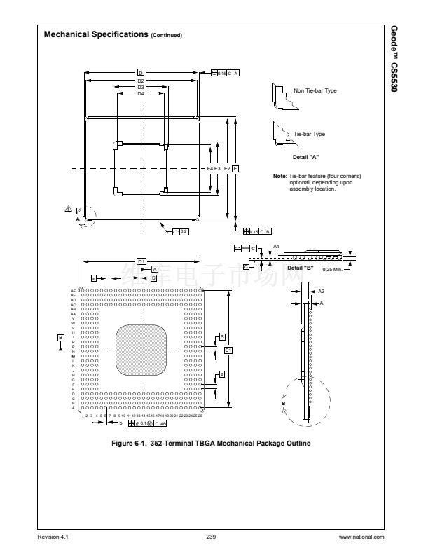
Geode鈩?CS5530
Functional Description
(Continued)
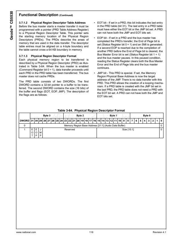
3.4.3.4 General Purpose I/O Pins
The CS5530 provides up to eight GPIO (general purpose
I/O) pins. Five of the pins (GPIO[7:4] and GPIO1) have
alternate functions. Table 3-30 shows the bits used for
GPIO pin function selection.
Each GPIO pin can be configured as an input or output.
GPIO[7:0] can be independently configured to act as
edge-sensitive SMI events. Each pin can be enabled and
configured to be either positive-edge sensitive or nega-
tive-edge sensitive. These pins then cause an SMI to be
generated when an appropriate edge condition is
detected. The power management status registers indi-
cate that a GPIO external SMI event has occurred.
The GPIO Pin Direction Register 1 (F0 Index 90h) selects
whether the GPIO pin is an input or output. The GPIO Pin
Data Register 1 (F0 Index 91h) contains the direct values
of the GPIO pins. Write operations are valid only for bits
defined as output. Reads from this register will read the
last written value if the pin is an output.
GPIO Control Register 1 (F0 Index 92h) configures the
operation of the GPIO pins for their various alternate func-
tions. Bits [5:3] set the edge sensitivity for generating an
SMI on the GPIO[2:0] (input) pins respectively. Bits [2:0]
enable the generation of an SMI. Bit 6 enables GPIO6 to
act as the lid switch input. Bit 7 determines which edge
transition will cause the General Purpose Timer 2 (F0
Index 8Ah) to reload.
Table 3-31 shows the bit formats for the GPIO pin configu-
ration and control registers.
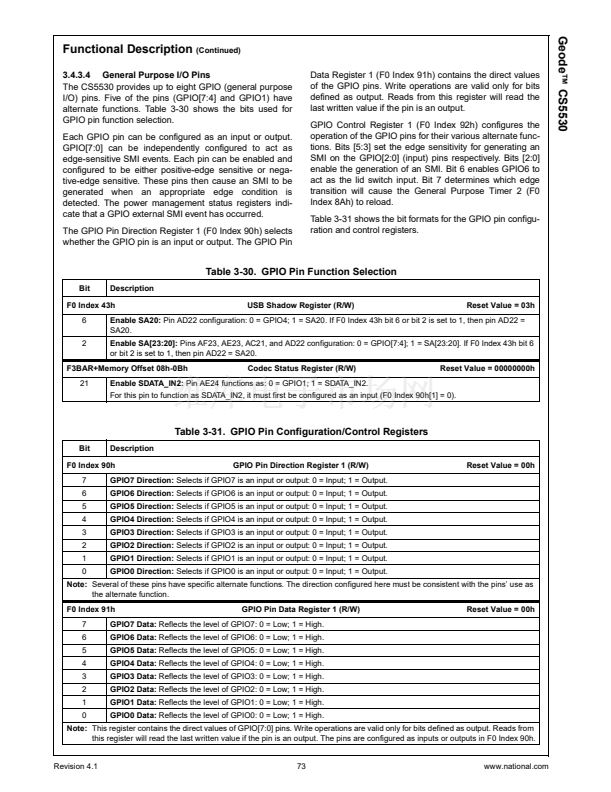
Table 3-30. GPIO Pin Function Selection
Bit
Description
USB Shadow Register (R/W)
Reset Value = 03h
F0 Index 43h
6
2
Enable SA20:
Pin AD22 configuration: 0 = GPIO4; 1 = SA20. If F0 Index 43h bit 6 or bit 2 is set to 1, then pin AD22 =
SA20.
Enable SA[23:20]:
Pins AF23, AE23, AC21, and AD22 configuration: 0 = GPIO[7:4]; 1 = SA[23:20]. If F0 Index 43h bit 6
or bit 2 is set to 1, then pin AD22 = SA20.
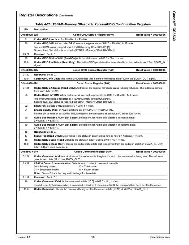
Codec Status Register (R/W)
Reset Value = 00000000h
F3BAR+Memory Offset 08h-0Bh
21
Enable SDATA_IN2:
Pin AE24 functions as: 0 = GPIO1; 1 = SDATA_IN2.
For this pin to function as SDATA_IN2, it must first be configured as an input (F0 Index 90h[1] = 0).
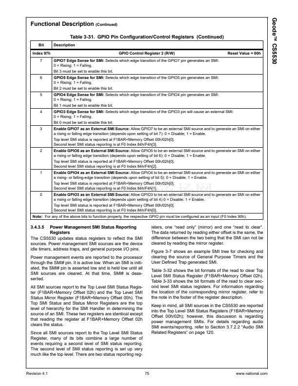
Table 3-31. GPIO Pin Configuration/Control Registers
Bit
Description
GPIO Pin Direction Register 1 (R/W)
Reset Value = 00h
F0 Index 90h
7
6
5
4
3
2
1
0
GPIO7 Direction:
Selects if GPIO7 is an input or output: 0 = Input; 1 = Output.
GPIO6 Direction:
Selects if GPIO6 is an input or output: 0 = Input; 1 = Output.
GPIO5 Direction:
Selects if GPIO5 is an input or output: 0 = Input; 1 = Output.
GPIO4 Direction:
Selects if GPIO4 is an input or output: 0 = Input; 1 = Output.
GPIO3 Direction:
Selects if GPIO3 is an input or output: 0 = Input; 1 = Output.
GPIO2 Direction:
Selects if GPIO2 is an input or output: 0 = Input; 1 = Output.
GPIO1 Direction:
Selects if GPIO1 is an input or output: 0 = Input; 1 = Output.
GPIO0 Direction:
Selects if GPIO0 is an input or output: 0 = Input; 1 = Output.
Note:
Several of these pins have specific alternate functions. The direction configured here must be consistent with the pins鈥?use as
the alternate function.
F0 Index 91h
7
6
5
4
3
2
1
0
GPIO Pin Data Register 1 (R/W)
Reset Value = 00h
GPIO7 Data:
Reflects the level of GPIO7: 0 = Low; 1 = High.
GPIO6 Data:
Reflects the level of GPIO6: 0 = Low; 1 = High.
GPIO5 Data:
Reflects the level of GPIO5: 0 = Low; 1 = High.
GPIO4 Data:
Reflects the level of GPIO4: 0 = Low; 1 = High.
GPIO3 Data:
Reflects the level of GPIO3: 0 = Low; 1 = High.
GPIO2 Data:
Reflects the level of GPIO2: 0 = Low; 1 = High.
GPIO1 Data:
Reflects the level of GPIO1: 0 = Low; 1 = High.
GPIO0 Data:
Reflects the level of GPIO0: 0 = Low; 1 = High.
Note:
This register contains the direct values of GPIO[7:0] pins. Write operations are valid only for bits defined as output. Reads from
this register will read the last written value if the pin is an output. The pins are configured as inputs or outputs in F0 Index 90h.
Revision 4.1
73
www.national.com


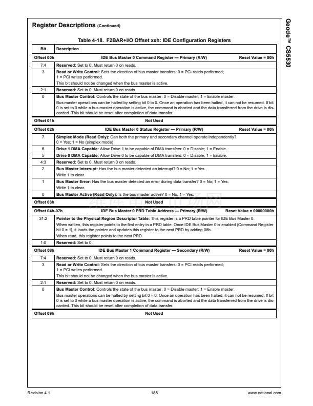
 1
1
 2
2
 3
3
 4
4
 5
5
 6
6
 7
7
 8
8
 9
9
 10
10
 11
11
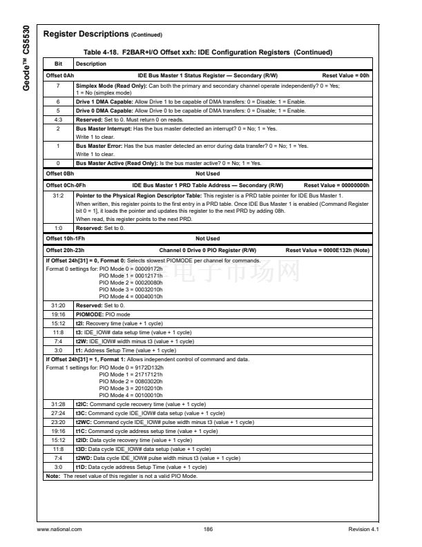
 12
12
 13
13
 14
14
 15
15
 16
16
 17
17
 18
18
 19
19
 20
20
 21
21
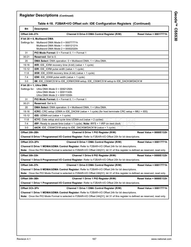
 22
22
 23
23
 24
24
 25
25
 26
26
 27
27
 28
28
 29
29
 30
30
 31
31
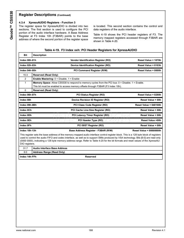
 32
32
 33
33
 34
34
 35
35
 36
36
 37
37
 38
38
 39
39
 40
40
 41
41
 42
42
 43
43
 44
44
 45
45
 46
46
 47
47
 48
48
 49
49
 50
50
 51
51
 52
52
 53
53
 54
54
 55
55
 56
56
 57
57
 58
58
 59
59
 60
60
 61
61
 62
62
 63
63
 64
64
 65
65
 66
66
 67
67
 68
68
 69
69
 70
70
 71
71
 72
72
 73
73
 74
74
 75
75
 76
76
 77
77
 78
78
 79
79
 80
80
 81
81
 82
82
 83
83
 84
84
 85
85
 86
86
 87
87
 88
88
 89
89
 90
90
 91
91
 92
92
 93
93
 94
94
 95
95
 96
96
 97
97
 98
98
 99
99
 100
100
 101
101
 102
102
 103
103
 104
104
 105
105
 106
106
 107
107
 108
108
 109
109
 110
110
 111
111
 112
112
 113
113
 114
114
 115
115
 116
116
 117
117
 118
118
 119
119
 120
120
 121
121
 122
122
 123
123
 124
124
 125
125
 126
126
 127
127
 128
128
 129
129
 130
130
 131
131
 132
132
 133
133
 134
134
 135
135
 136
136
 137
137
 138
138
 139
139
 140
140
 141
141
 142
142
 143
143
 144
144
 145
145
 146
146
 147
147
 148
148
 149
149
 150
150
 151
151
 152
152
 153
153
 154
154
 155
155
 156
156
 157
157
 158
158
 159
159
 160
160
 161
161
 162
162
 163
163
 164
164
 165
165
 166
166
 167
167
 168
168
 169
169
 170
170
 171
171
 172
172
 173
173
 174
174
 175
175
 176
176
 177
177
 178
178
 179
179
 180
180
 181
181
 182
182
 183
183
 184
184
 185
185
 186
186
 187
187
 188
188
 189
189
 190
190
 191
191
 192
192
 193
193
 194
194
 195
195
 196
196
 197
197
 198
198
 199
199
 200
200
 201
201
 202
202
 203
203
 204
204
 205
205
 206
206
 207
207
 208
208
 209
209
 210
210
 211
211
 212
212
 213
213
 214
214
 215
215
 216
216
 217
217
 218
218
 219
219
 220
220
 221
221
 222
222
 223
223
 224
224
 225
225
 226
226
 227
227
 228
228
 229
229
 230
230
 231
231
 232
232
 233
233
 234
234
 235
235
 236
236
 237
237
 238
238
 239
239
 240
240
 241
241
