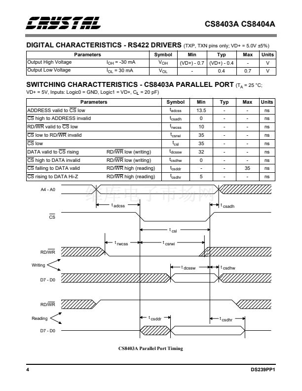
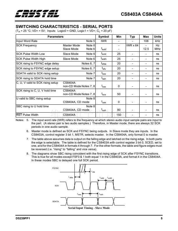
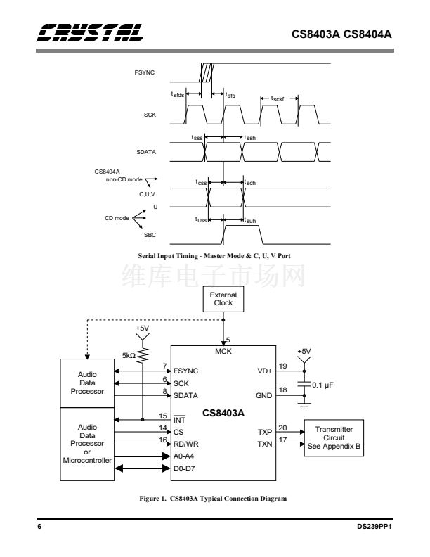
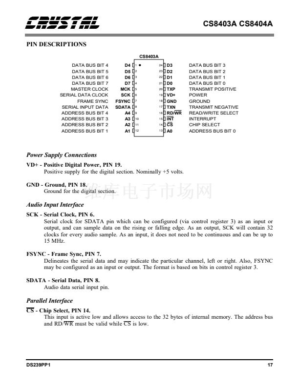
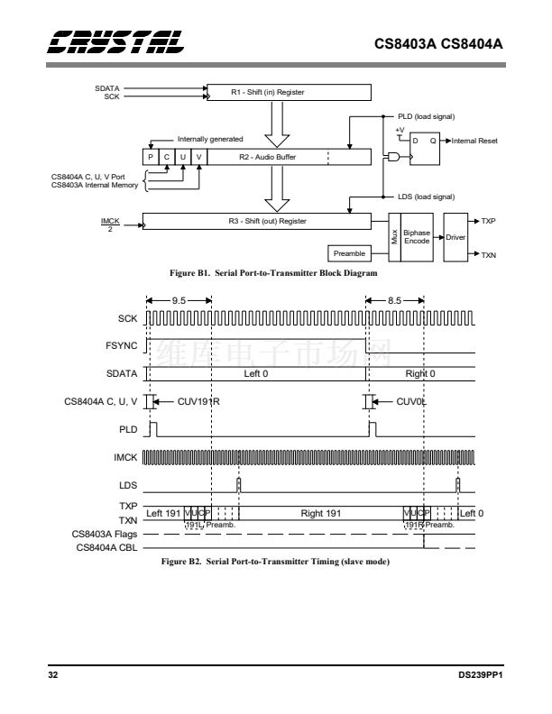
CS8403A CS8404A
SCK periods per sample respectively. As a master,
32 SCK periods are output per sample.
FSYNC must be derived from MCK via a DSP us-
ing the same clock or by external counters. If
FSYNC moves (jitters) with respect to MCK by
more than 4 MCK periods, the CS8403A may reset
the channel status block and flags. Appendix C
contains more information on the relationship of
FSYNC and MCK.
bit shift register which is shifted once per audio
sample. (An audio sample is defined as a single
channel, not a stereo pair.) The byte is transmitted
LSB first, D0 being the first bit. After transmitting
8 samples, i.e. 8 user bits, the address pointer is in-
cremented and the next byte of user data is loaded
into the shift register. After transmitting all four
bytes, 32 audio samples, the user read pointer is re-
set to 04H (Hex) and the cycle repeats.
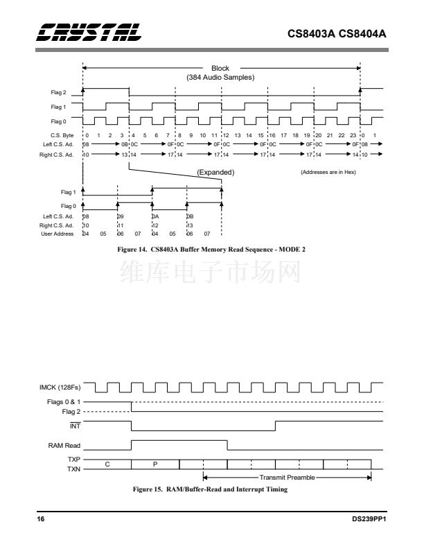
Flag 0 in the status register monitors the position of
the internal user data read pointer. When the first
byte, location 04H, is read, flag 0 is set low and
when the third byte, location 06H, is read, flag 0 is
set high. If mask 0 in control register1 is set, a tran-
sition of flag 0 will generate a low pulse on the in-
terrupt pin. The value of flag 0 indicates which two
bytes the part will read next, thereby indicating
which two bytes are free to be updated.
Flag 1 is mode dependent, changing with buffer
memory configuration, and is discussed in the indi-
vidual buffer mode sections.
Buffer Memory
In all buffer modes, the status register and control
registers are located at addresses 0-3 respectively,
and the user data is buffered in locations 4-7. The
parallel port can access any location in the user data
buffer at any time; however, care must be taken not
to modify a location when that location is being
read internally. This internal reading is done
through the second port of the buffer in a cyclic
manner.
Reset initializes the internal pointer to 04H(Hex).
Data is read from this location and stored in an 8-
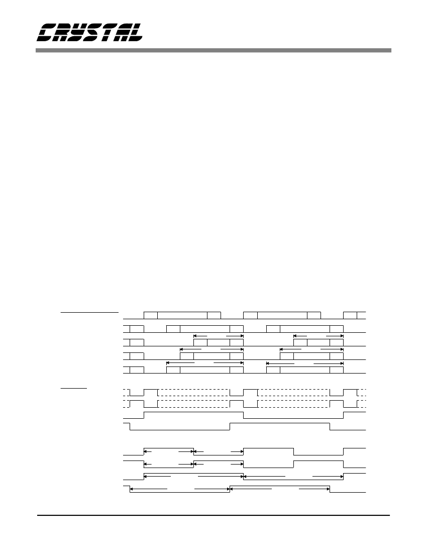
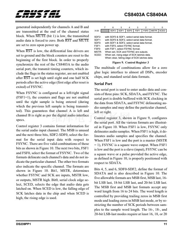
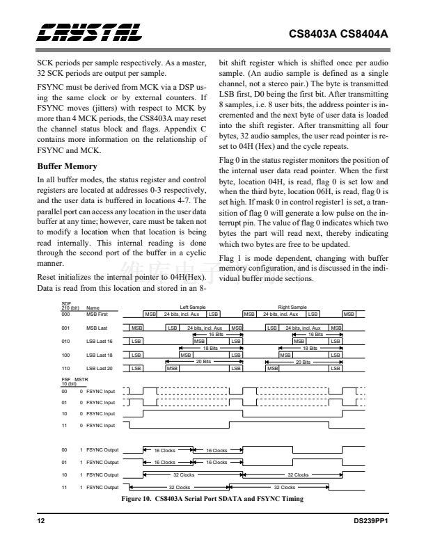
SDF
210 (bit)
000
Name
MSB First
MSB
Left Sample
LSB
24 bits, incl. Aux
MSB
Right Sample
LSB
24 bits, incl. Aux
MSB
001
010
100
110
MSB Last
LSB Last 16
LSB Last 18
LSB Last 20
MSB
LSB
LSB
LSB
LSB
24 bits, incl. Aux
16 Bits
MSB
18 Bits
MSB
20 Bits
MSB
LSB
LSB
LSB
LSB
24 bits, incl. Aux
16 Bits
MSB
18 Bits
MSB
20 Bits
MSB
LSB
LSB
LSB
MSB
MSB
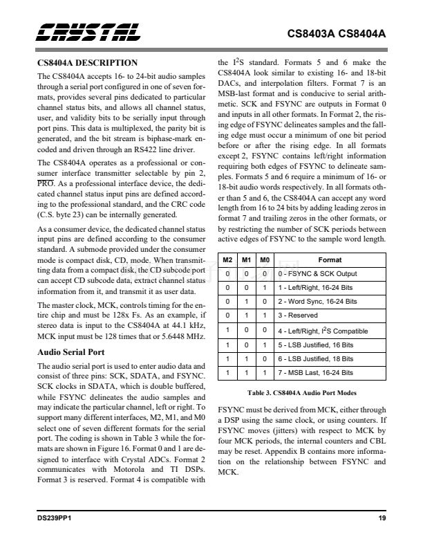
FSF MSTR
10 (bit)
00
01
10
0 FSYNC Input
0 FSYNC Input
0 FSYNC Input
11
0 FSYNC Input
00
01
10
11
1 FSYNC Output
1 FSYNC Output
1 FSYNC Output
1 FSYNC Output
16 Clocks
16 Clocks
16 Clocks
32 Clocks
32 Clocks
16 Clocks
32 Clocks
32 Clocks
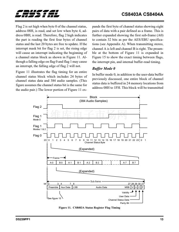
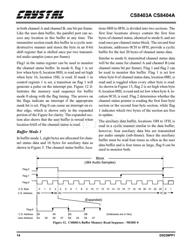
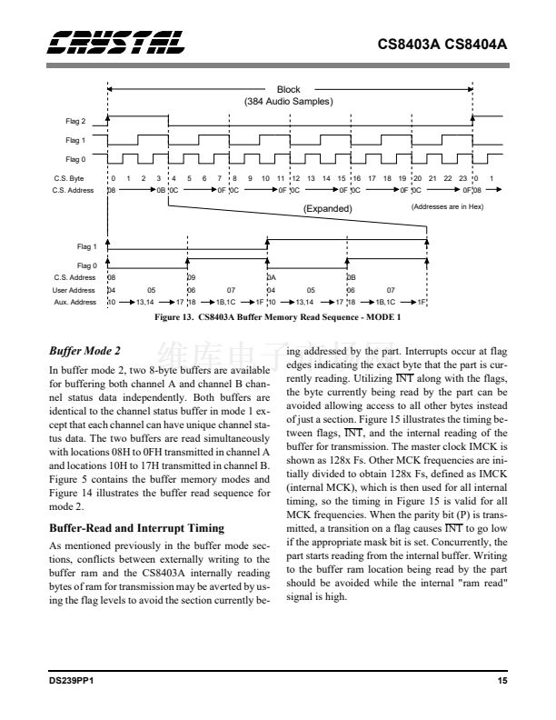
Figure 10. CS8403A Serial Port SDATA and FSYNC Timing
12
DS239PP1


 1
1
 2
2
 3
3
 4
4
 5
5
 6
6
 7
7
 8
8
 9
9
 10
10
 11
11
 12
12
 13
13
 14
14
 15
15
 16
16
 17
17
 18
18
 19
19
 20
20
 21
21
 22
22
 23
23
 24
24
 25
25
 26
26
 27
27
 28
28
 29
29
 30
30
 31
31
 32
32
 33
33
