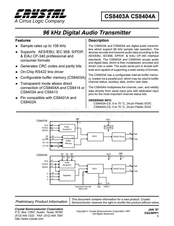
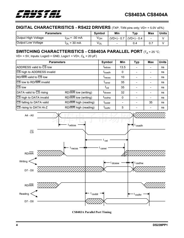
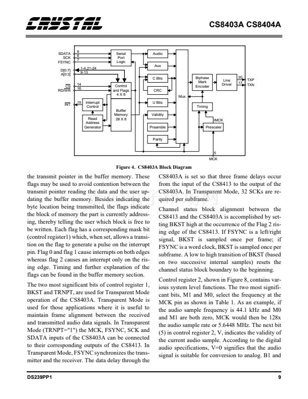
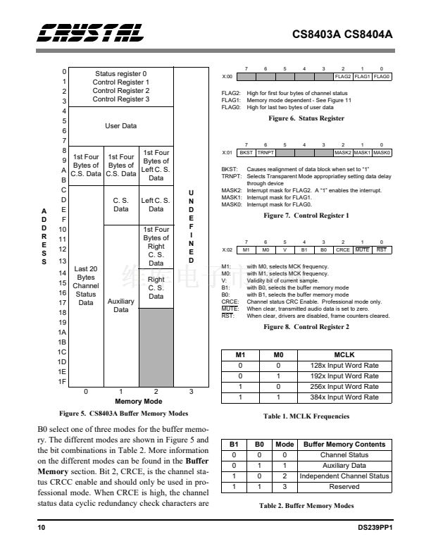
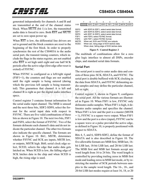
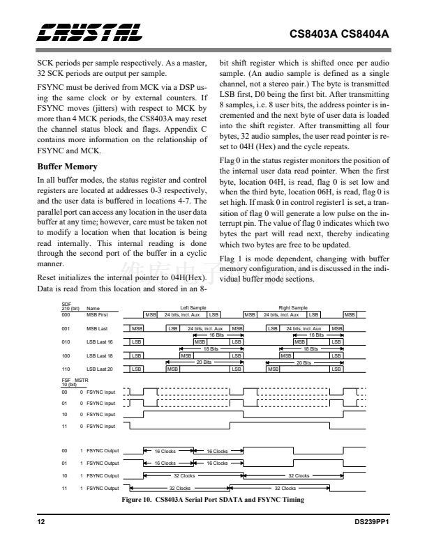
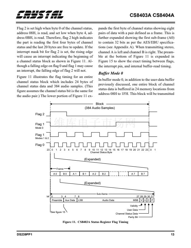
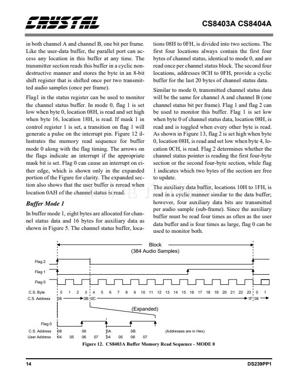
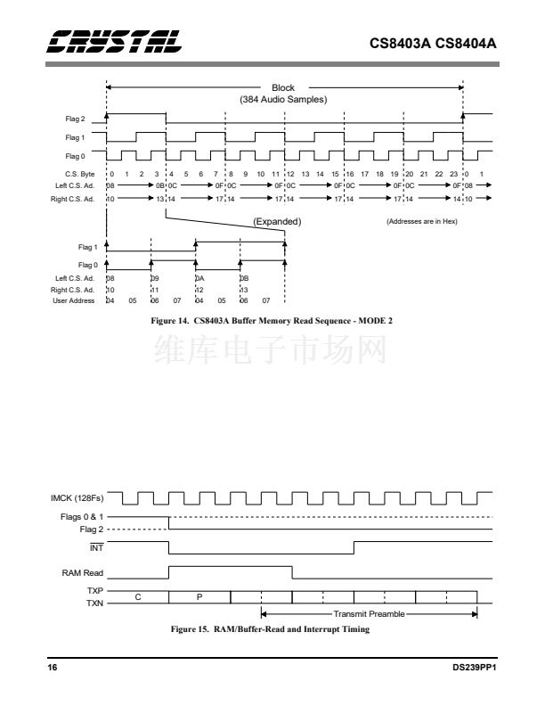
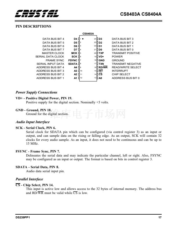
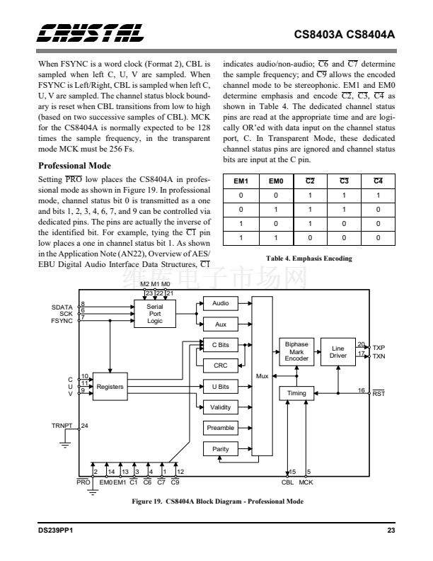
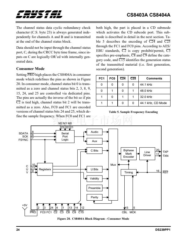
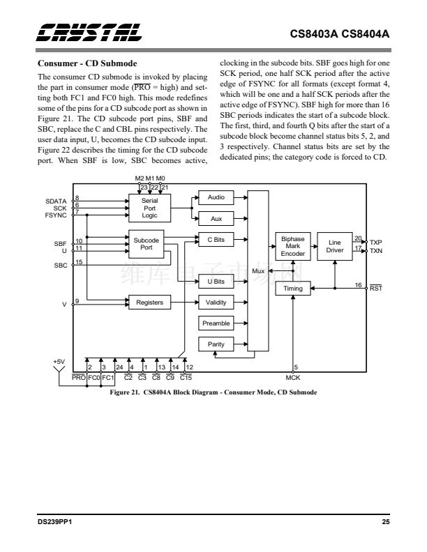
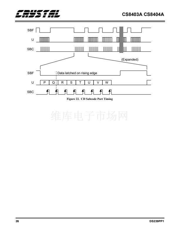
CS8403A CS8404A
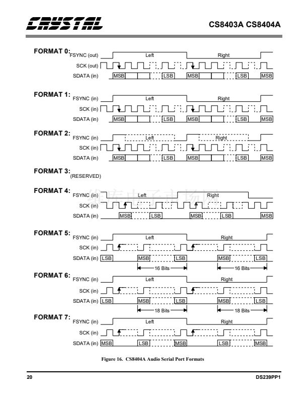
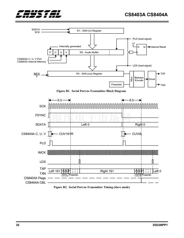
C, U, V Serial Port
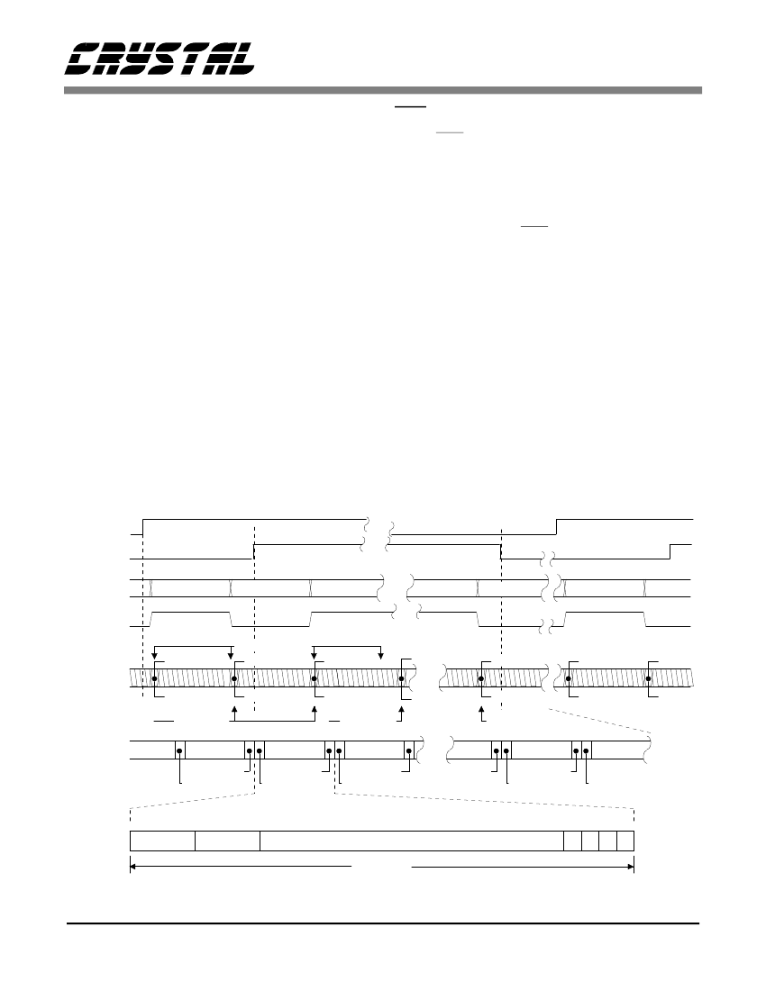
The serial input pins for channel status (C), user
(U), and validity (V) are sampled during the first bit
period after the active edge of FSYNC for all for-
mats except Format 4. Format 4 is sampled during
the second bit period (coincident with the MSB). In
Figure 16, the arrows on SCK indicate when the C,
U, and V bits are sampled. The C, U, and V bits are
transmitted with the audio sample entered before
the FSYNC edge that sampled it. The V bit, as de-
fined in the audio standards, is set to zero to indi-
cate the audio data is suitable for conversion to
analog. Therefore, when the audio data is errorred,
or the data is not audio, the V bit should be set high.
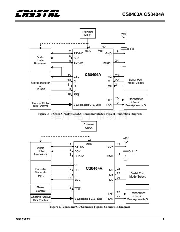
The channel status serial input pin (C) is not avail-
able in consumer mode when the CD subcode port
is enabled (FC1 = FC0 = high). Any channel status
data entered through the channel status serial input
(C) is logically OR鈥檈d with the data entered
through the dedicated pins or internally generated.
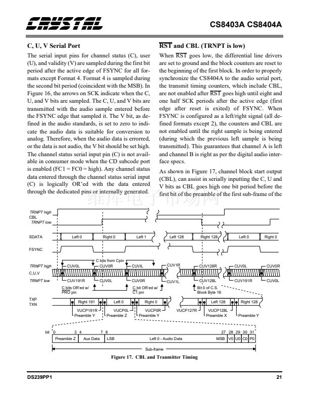
RST and CBL (TRNPT is low)
When RST goes low, the differential line drivers
are set to ground and the block counters are reset to
the beginning of the first block. In order to properly
synchronize the CS8404A to the audio serial port,
the transmit timing counters, which include CBL,
are not enabled after RST goes high until eight and
one half SCK periods after the active edge (first
edge after reset is exited) of FSYNC. When
FSYNC is configured as a left/right signal (all de-
fined formats except 2), the counters and CBL are
not enabled until the right sample is being entered
(during which the previous left sample is being
transmitted). This guarantees that channel A is left
and channel B is right as per the digital audio inter-
face specs.
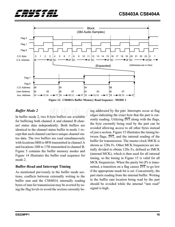
As shown in Figure 17, channel block start output
(CBL), can assist in serially inputting the C, U and
V bits as CBL goes high one bit period before the
first bit of the preamble of the first sub-frame of the
TRNPT high
CBL
TRNPT low
SDATA
FSYNC
Left 0
Right 0
Left 1
Left 128
Right 128
Left 0
Right 0
TRNPT high
C,U,V
CUV0L
C bits from Cpin
CUV0R
CUVIL
CUV1R
CUV128R
CUV0L
CUV0R
TRNPT low
CUV191R
C bits OR鈥檈d w/
PRO pin
CUV0L
CUV0R
C bit OR鈥檈d w/
C1 pin
Left 0
Right 0
VUCP0R
Preamble Y
CUV1L
CUV128L
Bit 0 of C.S.
Block Byte 16
Left 128
CUV191R
CUV0L
TXP
TXN
Right 191
VUCP191R
Preamble Y
Right 128
VUCP0L
Preamble Z
VUCP127R
VUCP128L
Preamble X
Preamble Y
bit 0
3 4
Aux Data
7 8
LSB
Left 0 - Audio Data
27 28 29 30 31
MSB V0 U0 C0 P0
Preamble Z
Sub-frame
Figure 17. CBL and Tranmitter Timing
DS239PP1
21


 1
1
 2
2
 3
3
 4
4
 5
5
 6
6
 7
7
 8
8
 9
9
 10
10
 11
11
 12
12
 13
13
 14
14
 15
15
 16
16
 17
17
 18
18
 19
19
 20
20
 21
21
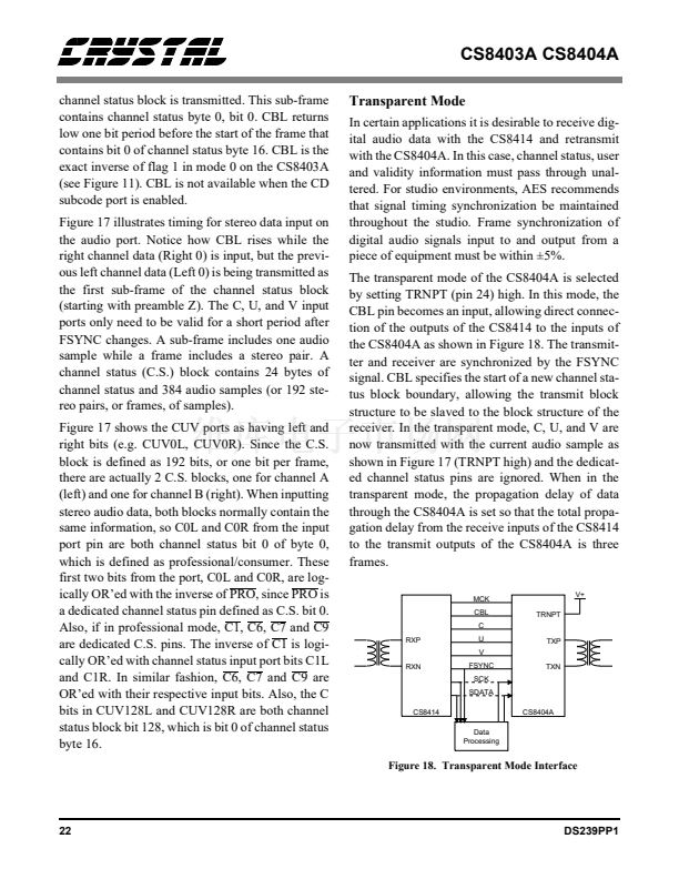 22
22
 23
23
 24
24
 25
25
 26
26
 27
27
 28
28
 29
29
 30
30
 31
31
 32
32
 33
33
