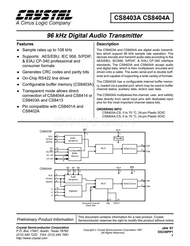
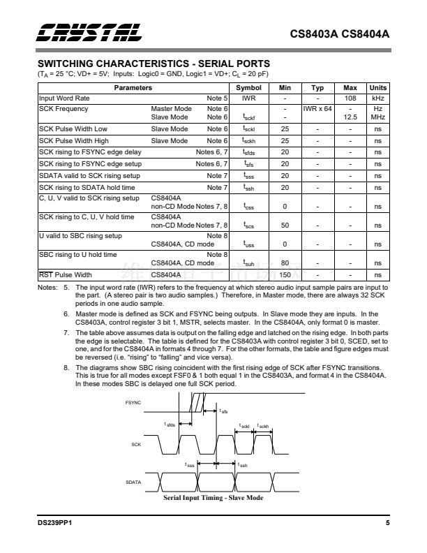
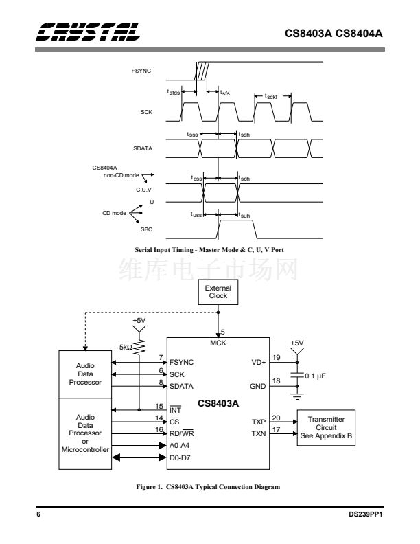
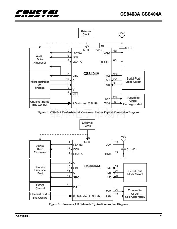
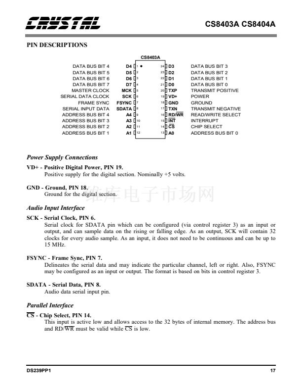
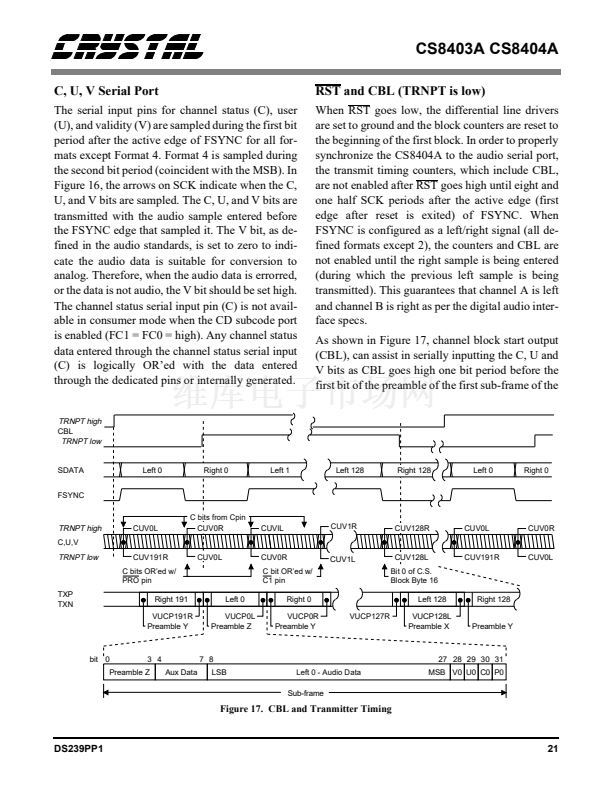
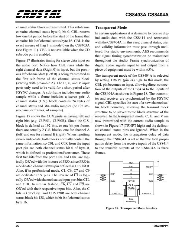
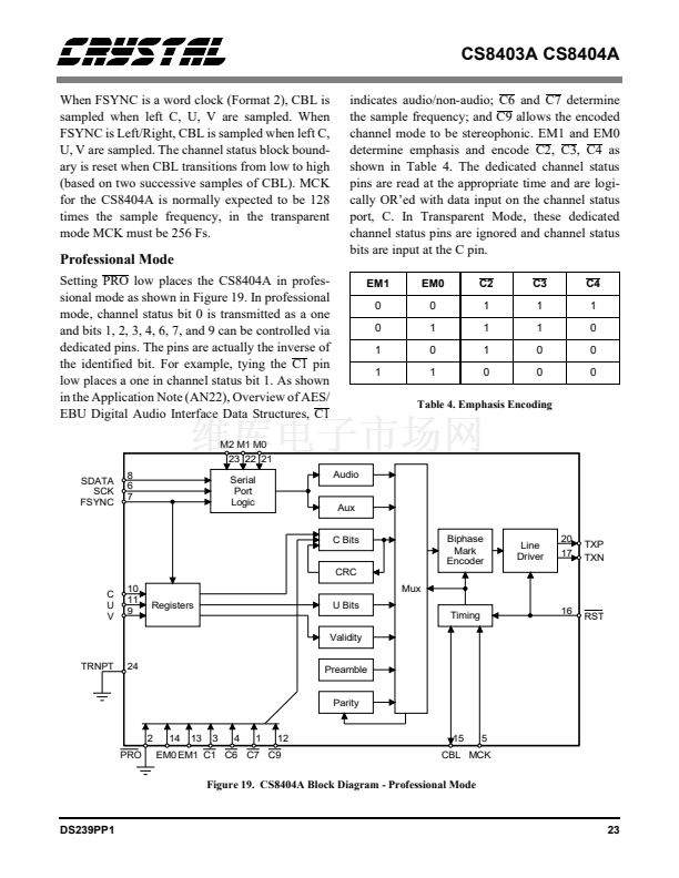
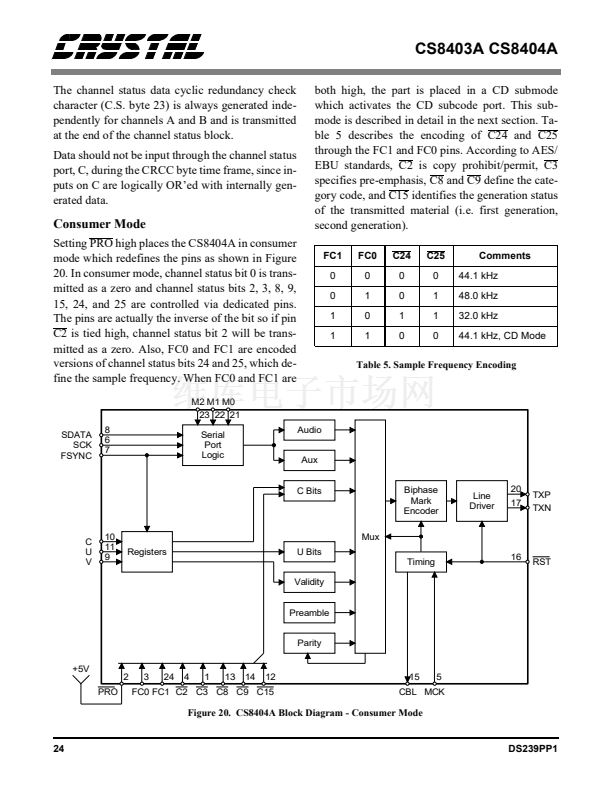
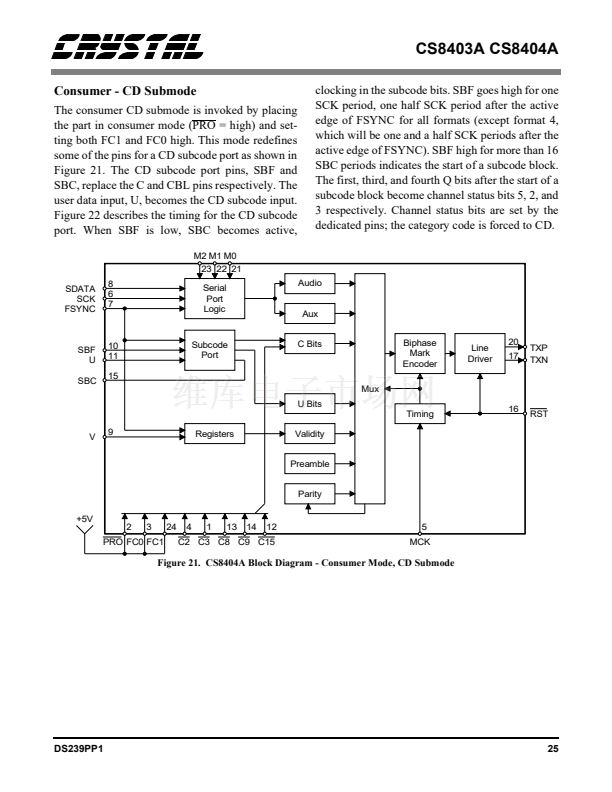
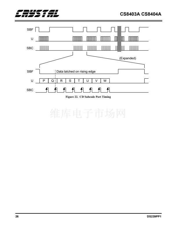
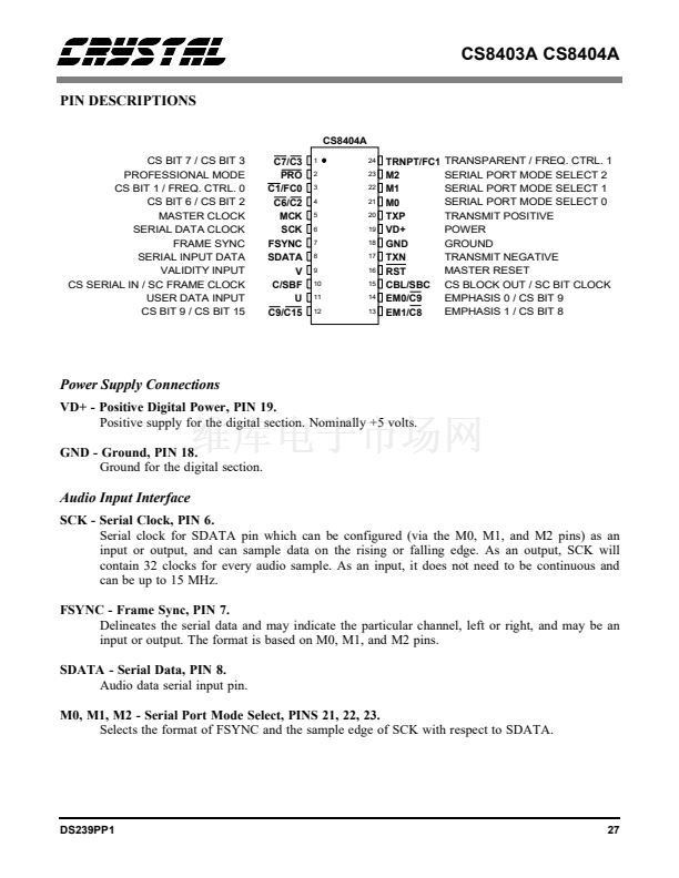
CS8403A CS8404A
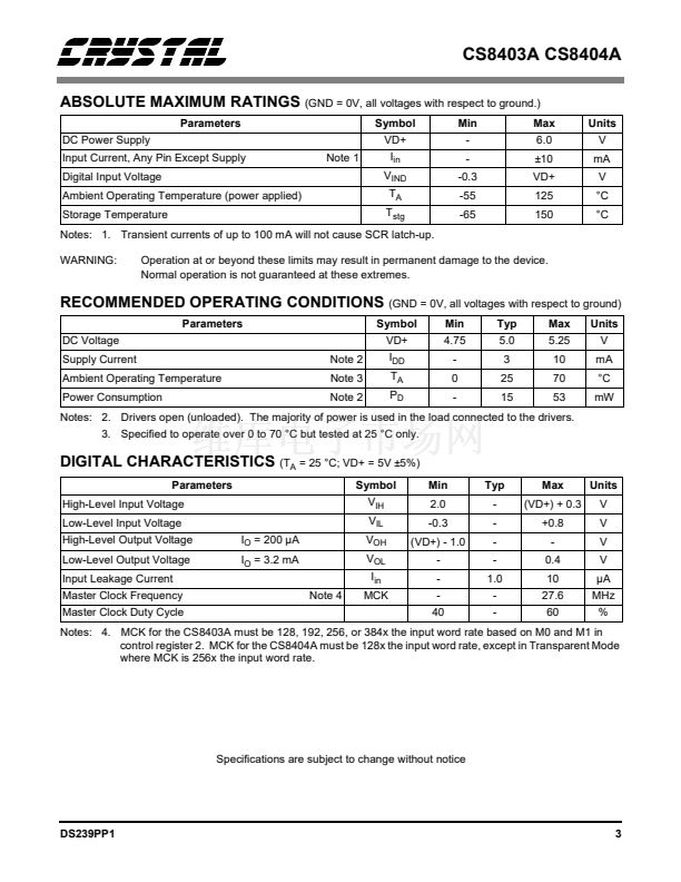
ABSOLUTE MAXIMUM RATINGS
(GND = 0V, all voltages with respect to ground.)
Parameters
DC Power Supply
Input Current, Any Pin Except Supply
Digital Input Voltage
Ambient Operating Temperature (power applied)
Storage Temperature
Note 1
Symbol
VD+
I
in
V
IND
T
A
T
stg
Min
-
-
-0.3
-55
-65
Max
6.0
卤10
VD+
125
150
Units
V
mA
V
掳C
掳C
Notes: 1. Transient currents of up to 100 mA will not cause SCR latch-up.
WARNING:
Operation at or beyond these limits may result in permanent damage to the device.
Normal operation is not guaranteed at these extremes.
RECOMMENDED OPERATING CONDITIONS
(GND = 0V, all voltages with respect to ground)
Parameters
DC Voltage
Supply Current
Ambient Operating Temperature
Power Consumption
Note 2
Note 3
Note 2
Symbol
VD+
I
DD
T
A
P
D
Min
4.75
-
0
-
Typ
5.0
3
25
15
Max
5.25
10
70
53
Units
V
mA
掳C
mW
Notes: 2. Drivers open (unloaded). The majority of power is used in the load connected to the drivers.
3. Specified to operate over 0 to 70 掳C but tested at 25 掳C only.
DIGITAL CHARACTERISTICS
(T
A
= 25 掳C; VD+ = 5V 卤5%)
Parameters
High-Level Input Voltage
Low-Level Input Voltage
High-Level Output Voltage
Low-Level Output Voltage
Input Leakage Current
Master Clock Frequency
Master Clock Duty Cycle
Note 4
I
O
= 200 碌A
I
O
= 3.2 mA
Symbol
V
IH
V
IL
V
OH
V
OL
I
in
MCK
Min
2.0
-0.3
(VD+) - 1.0
-
-
-
40
Typ
-
-
-
-
1.0
-
-
Max
(VD+) + 0.3
+0.8
-
0.4
10
27.6
60
Units
V
V
V
V
碌A
MHz
%
Notes: 4. MCK for the CS8403A must be 128, 192, 256, or 384x the input word rate based on M0 and M1 in
control register 2. MCK for the CS8404A must be 128x the input word rate, except in Transparent Mode
where MCK is 256x the input word rate.
Specifications are subject to change without notice
DS239PP1
3


 1
1
 2
2
 3
3
 4
4
 5
5
 6
6
 7
7
 8
8
 9
9
 10
10
 11
11
 12
12
 13
13
 14
14
 15
15
 16
16
 17
17
 18
18
 19
19
 20
20
 21
21
 22
22
 23
23
 24
24
 25
25
 26
26
 27
27
 28
28
 29
29
 30
30
 31
31
 32
32
 33
33
