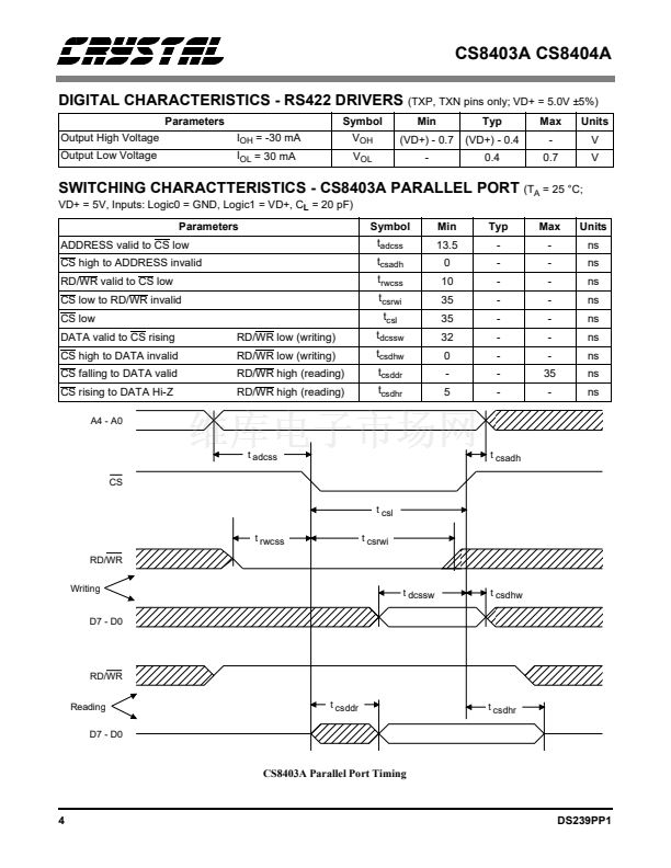
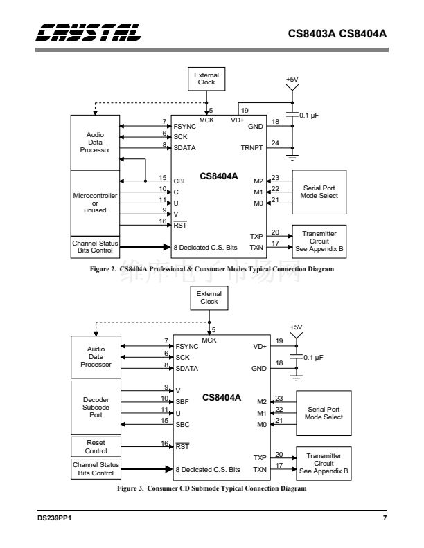
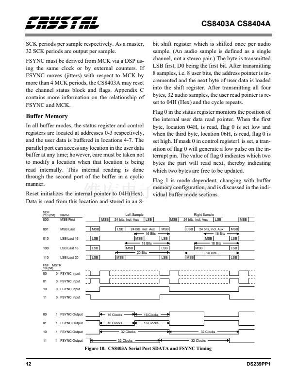
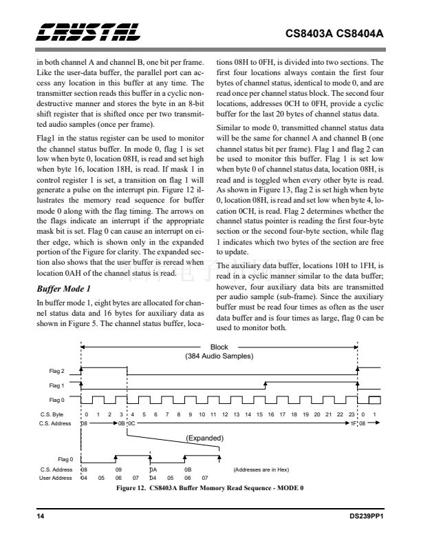
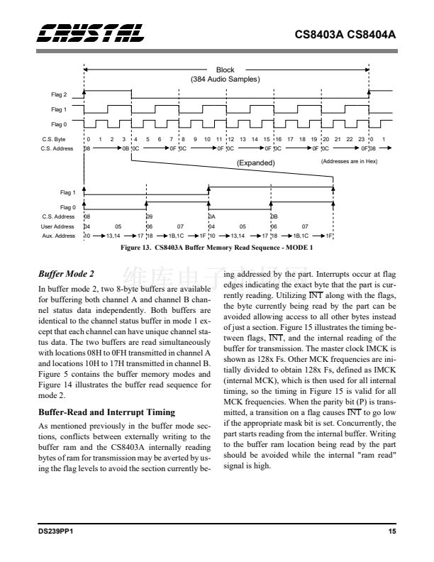
CS8403A CS8404A
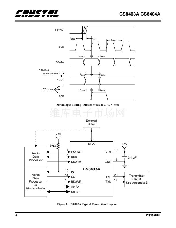
External
Clock
+5V
7
Audio
Data
Processor
6
8
5
MCK
FSYNC
SCK
SDATA
19
VD+
GND
TRNPT
0.1 碌F
18
24
15
10
Microcontroller
or
unused
11
9
16
CBL
CS8404A
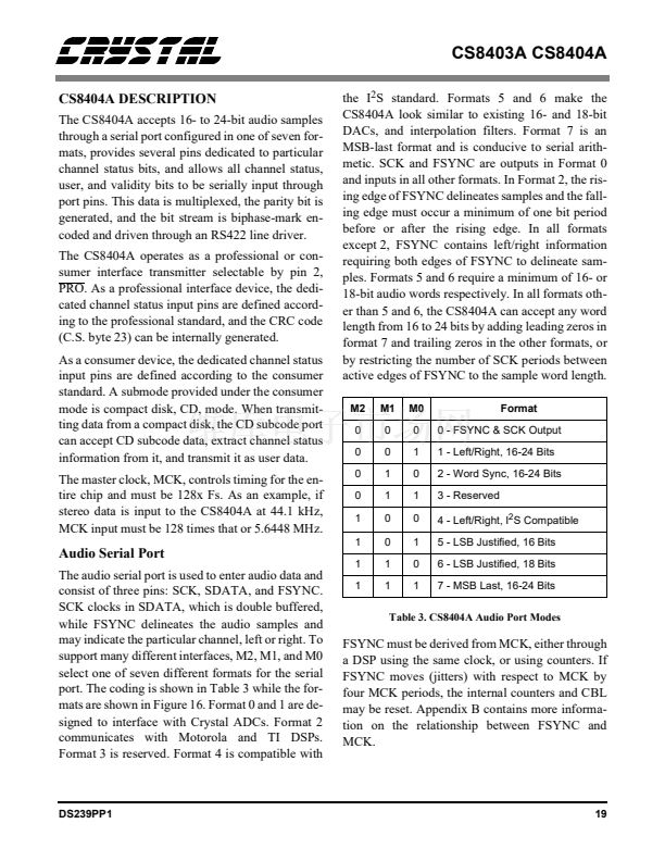
M2
23
22
21
Serial Port
Mode Select
C
U
V
RST
M1
M0
TXP
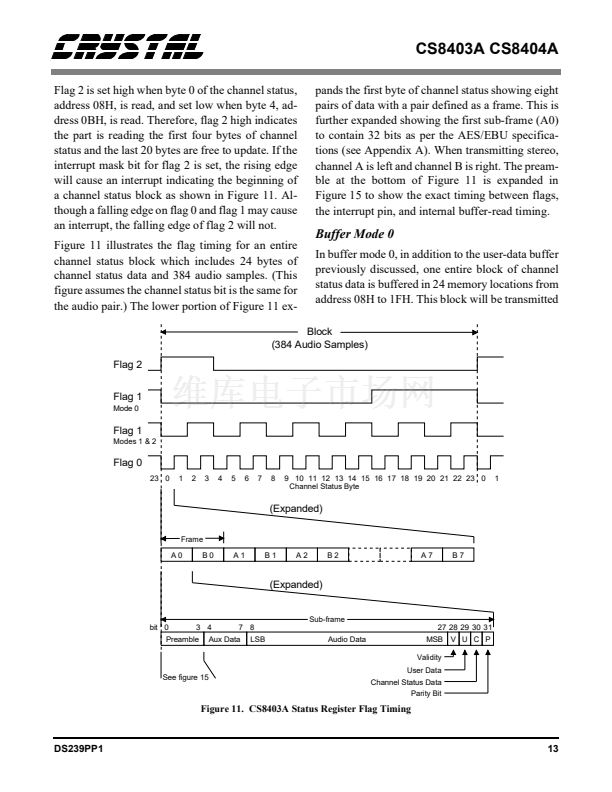
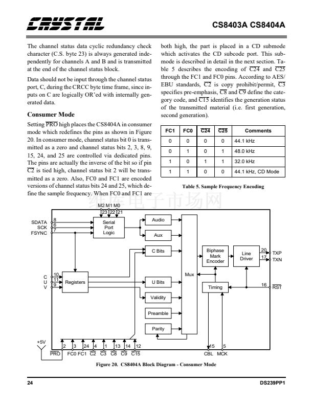
Channel Status
Bits Control
8 Dedicated C.S. Bits
TXN
20
17
Transmitter
Circuit
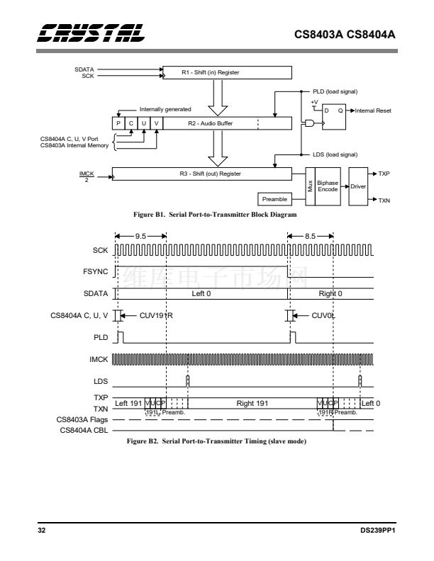
See Appendix B
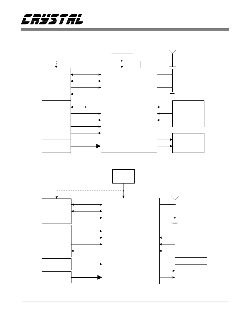
Figure 2. CS8404A Professional & Consumer Modes Typical Connection Diagram
External
Clock
7
Audio
Data
Processor
6
8
9
Decoder
Subcode
Port
10
11
15
16
5
MCK
FSYNC
SCK
SDATA
V
SBF
+5V
VD+
GND
19
0.1 碌F
18
CS8404A
M2
23
22
21
Serial Port
Mode Select
U
SBC
RST
M1
M0
Reset
Control
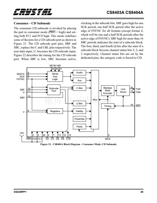
Channel Status
Bits Control
TXP
8 Dedicated C.S. Bits
TXN
20
17
Transmitter
Circuit
See Appendix B
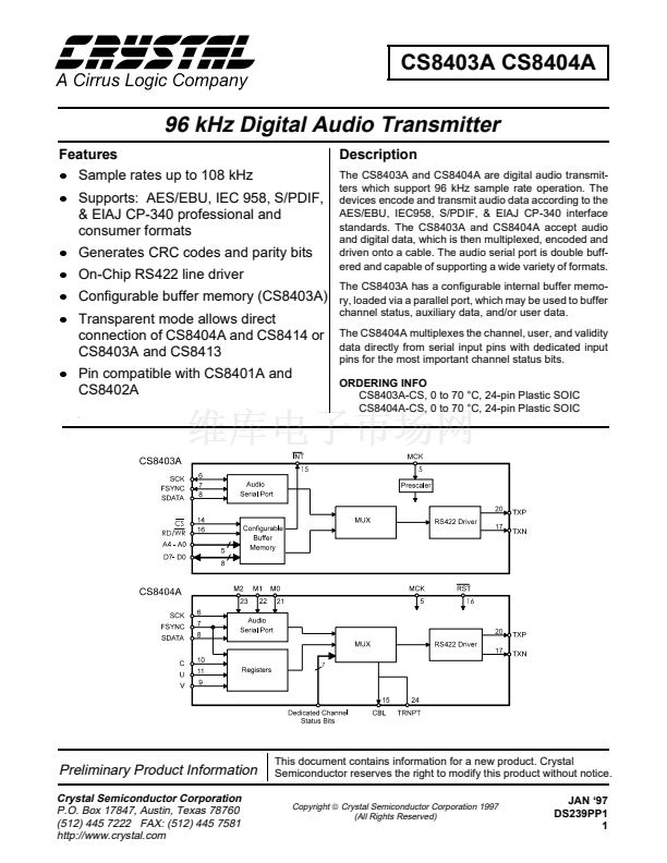
Figure 3. Consumer CD Submode Typical Connection Diagram
DS239PP1
7


 1
1
 2
2
 3
3
 4
4
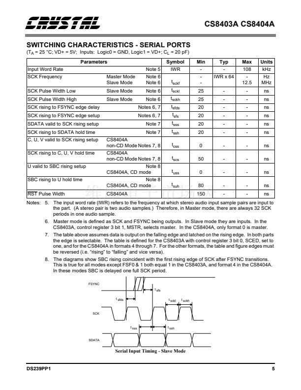 5
5
 6
6
 7
7
 8
8
 9
9
 10
10
 11
11
 12
12
 13
13
 14
14
 15
15
 16
16
 17
17
 18
18
 19
19
 20
20
 21
21
 22
22
 23
23
 24
24
 25
25
 26
26
 27
27
 28
28
 29
29
 30
30
 31
31
 32
32
 33
33
