Bits 15-0 are the 16-Bit conversion result MSB first.
Bit 0 is the least significant bit (LSB).
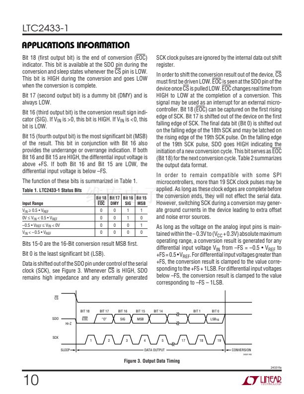
clock (SCK), see Figure 3. Whenever CS is HIGH, SDO
鈥淥鈥?/div>
BIT 16
SIG
SCK
1
SLEEP
2
Figure 3. Output Data Timing
24331fa
10
U
SCK clock pulses are ignored by the internal data out shift
register.
In order to shift the conversion result out of the device, CS
must first be driven LOW. EOC is seen at the SDO pin of the
device once CS is pulled LOW. EOC changes real time from
HIGH to LOW at the completion of a conversion. This
signal may be used as an interrupt for an external micro-
controller. Bit 18 (EOC) can be captured on the first rising
edge of SCK. Bit 17 is shifted out of the device on the first
falling edge of SCK. The final data bit (Bit 0) is shifted out
on the falling edge of the 18th SCK and may be latched on
the rising edge of the 19th SCK pulse. On the falling edge
of the 19th SCK pulse, SDO goes HIGH indicating the
initiation of a new conversion cycle. This bit serves as EOC
(Bit 18) for the next conversion cycle. Table 2 summarizes
the output data format.
In order to remain compatible with some SPI
microcontrollers, more than 19 SCK clock pulses may be
applied. As long as these clock edges are complete before
the conversion ends, they will not effect the serial data.
However, switching SCK during a conversion may gener-
ate ground currents in the device leading to extra offset
and noise error sources.
As long as the voltage on the analog input pins is main-
tained within the 鈥?0.3V to (V
CC
+ 0.3V) absolute maximum
operating range, a conversion result is generated for any
differential input voltage V
IN
from 鈥揊S = 鈥?.5 鈥?V
REF
to
+FS = 0.5 鈥?V
REF
. For differential input voltages greater than
+FS, the conversion result is clamped to the value corre-
sponding to the +FS + 1LSB. For differential input voltages
below 鈥揊S, the conversion result is clamped to the value
corresponding to 鈥揊S 鈥?1LSB.
BIT 15
MSB
BIT 14
BIT 1
BIT 0
LSB
16
3
4
5
17
18
19
CONVERSION
24331 F03
W
U U
DATA OUTPUT


 1
1
 2
2
 3
3
 4
4
 5
5
 6
6
 7
7
 8
8
 9
9
 10
10
 11
11
 12
12
 13
13
 14
14
 15
15
 16
16
 17
17
 18
18
 19
19
 20
20
 21
21
 22
22
 23
23
 24
24
 25
25
 26
26
 27
27
 28
28
