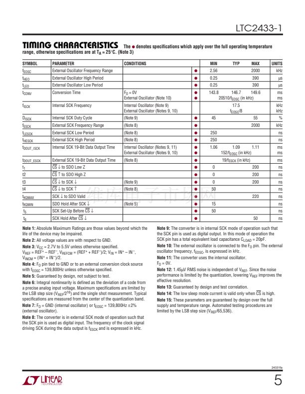
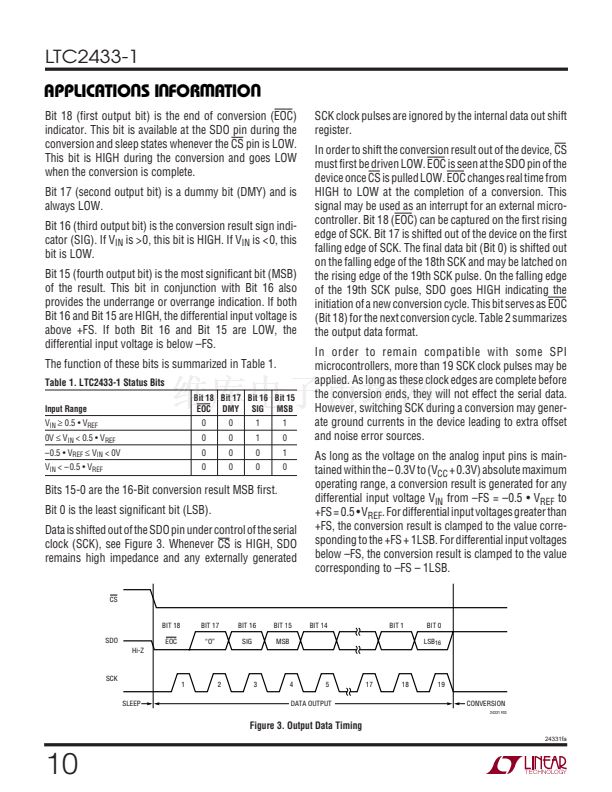
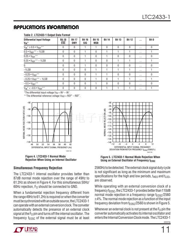
鈮?/div>
1碌F)
22
U
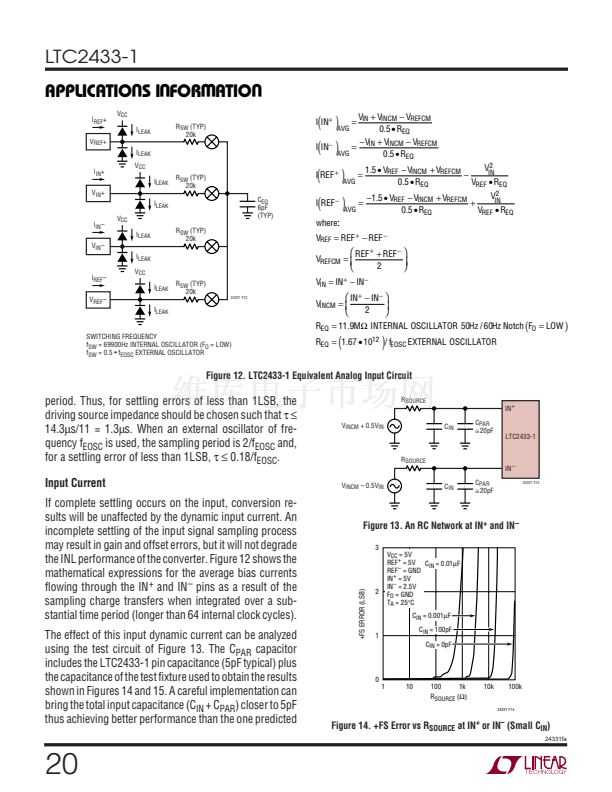
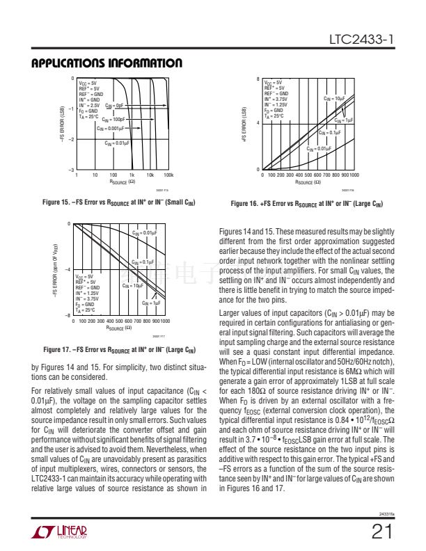
If possible, it is desirable to operate with the input signal
common mode voltage very close to the reference signal
common mode voltage as is the case in the ratiometric
measurement of a symmetric bridge. This configuration
eliminates the offset error caused by mismatched source
impedances.
The magnitude of the dynamic input current depends upon
the size of the very stable internal sampling capacitors and
upon the accuracy of the converter sampling clock. The
accuracy of the internal clock over the entire temperature
and power supply range is typically better than 0.5%. Such
a specification can also be easily achieved by an external
clock. When relatively stable resistors (50ppm/掳C) are
used for the external source impedance seen by IN
+
and
IN
鈥?/div>
, the expected drift of the dynamic current, offset and
gain errors will be insignificant (about 1% of their respec-
tive values over the entire temperature and voltage range).
Even for the most stringent applications, a one-time
calibration operation may be sufficient.
In addition to the input sampling charge, the input ESD
protection diodes have a temperature dependent leakage
current. This current, nominally 1nA (卤10nA max), results
in a small offset shift. A 15k source resistance will create
a 0LSB typical and 1LSB maximum offset voltage.
Reference Current
In a similar fashion, the LTC2433-1 samples the differen-
tial reference pins REF
+
and REF
鈥?/div>
transfering small amount
of charge to and from the external driving circuits thus
producing a dynamic reference current. This current does
not change the converter offset, but it may degrade the
gain and INL performance. The effect of this current can be
analyzed in the same two distinct situations.
For relatively small values of the external reference capaci-
tors (C
REF
< 0.01碌F), the voltage on the sampling capacitor
settles almost completely and relatively large values for
the source impedance result in only small errors. Such
values for C
REF
will deteriorate the converter offset and
gain performance without significant benefits of reference
filtering and the user is advised to avoid them.
24331fa
W
U U


 1
1
 2
2
 3
3
 4
4
 5
5
 6
6
 7
7
 8
8
 9
9
 10
10
 11
11
 12
12
 13
13
 14
14
 15
15
 16
16
 17
17
 18
18
 19
19
 20
20
 21
21
 22
22
 23
23
 24
24
 25
25
 26
26
 27
27
 28
28
