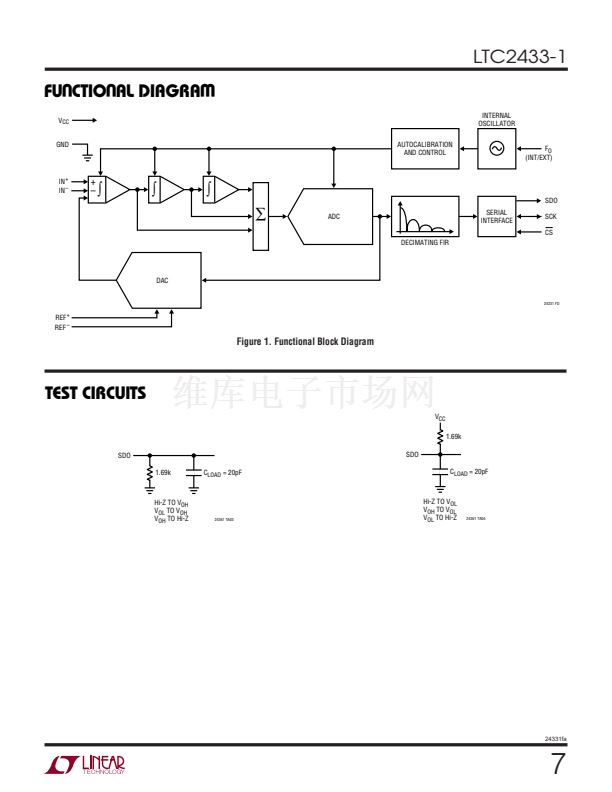
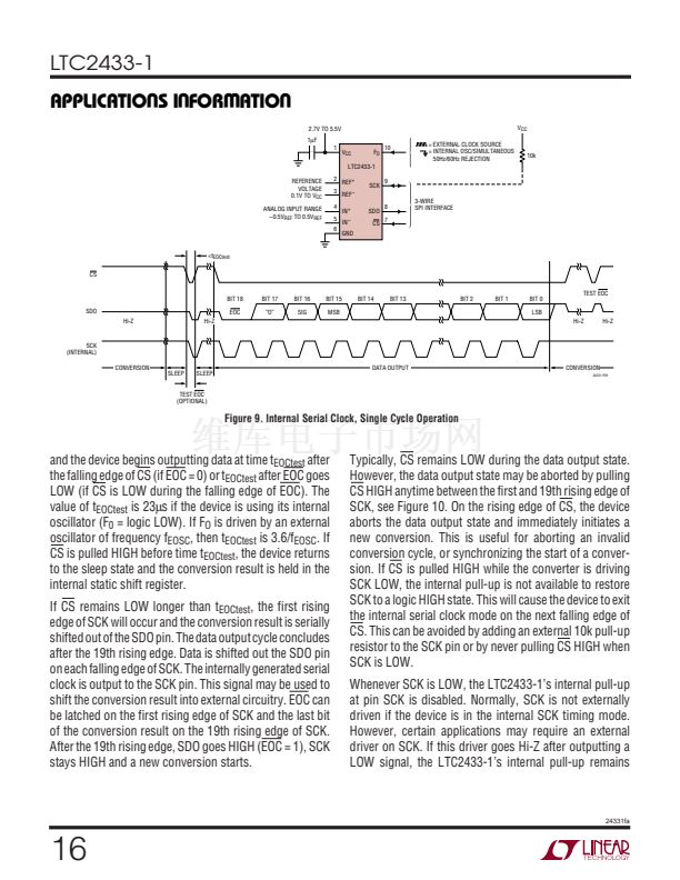
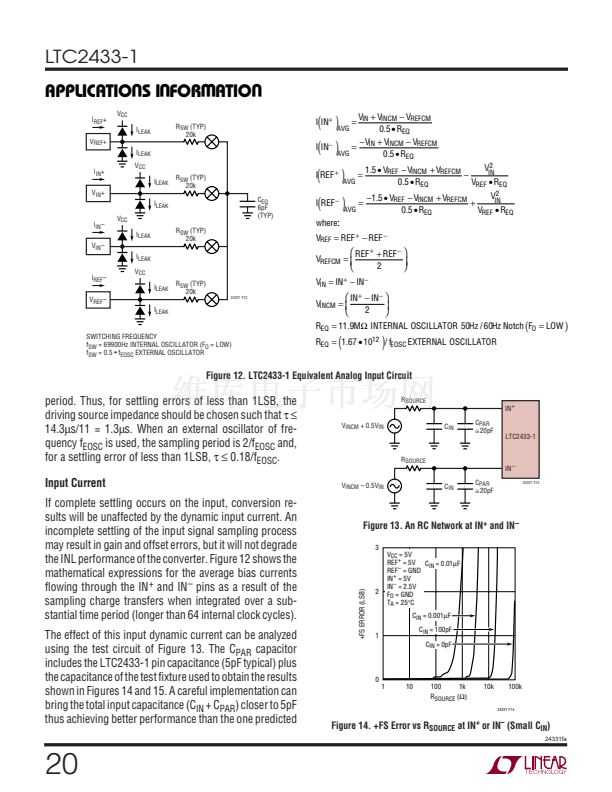
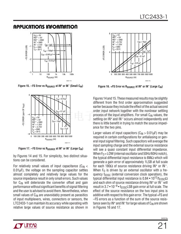
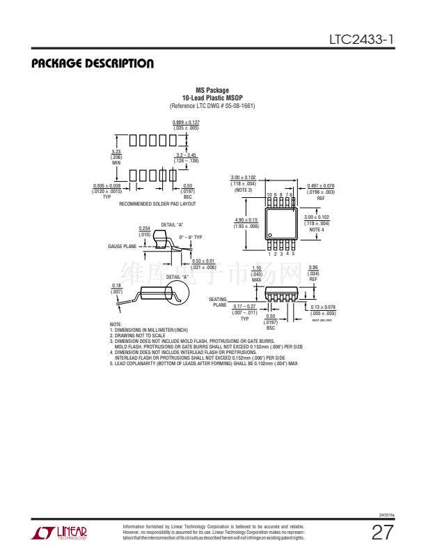
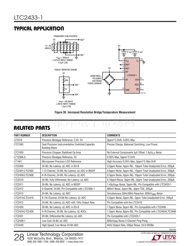
LTC2433-1
APPLICATIO S I FOR ATIO
operation will not be disturbed if the change of conversion
clock source occurs during the sleep state or during the
data output state while the converter uses an external
serial clock. If the change occurs during the conversion
state, the result of the conversion in progress may be
outside specifications but the following conversions will
not be affected. If the change occurs during the data output
state and the converter is in the Internal SCK mode, the
serial clock duty cycle may be affected but the serial data
stream will remain valid.
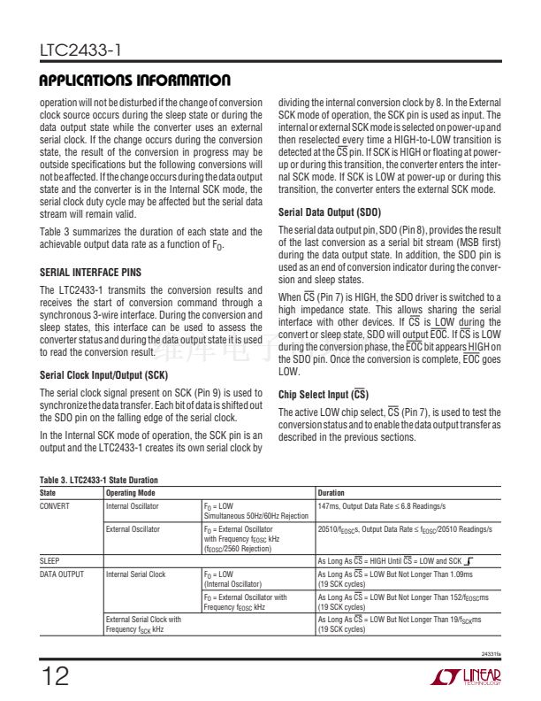
Table 3 summarizes the duration of each state and the
achievable output data rate as a function of F
O
.
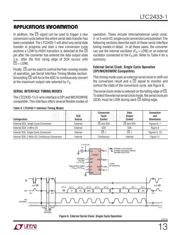
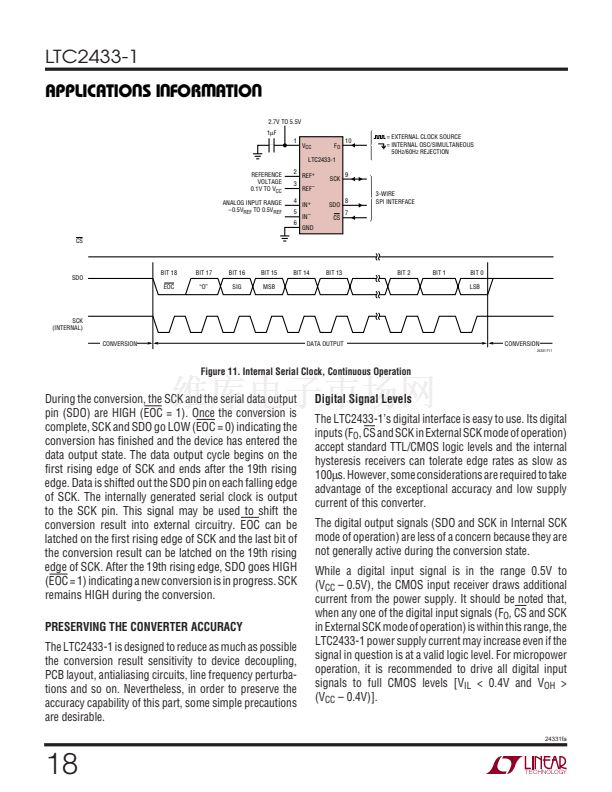
SERIAL INTERFACE PINS
The LTC2433-1 transmits the conversion results and
receives the start of conversion command through a
synchronous 3-wire interface. During the conversion and
sleep states, this interface can be used to assess the
converter status and during the data output state it is used
to read the conversion result.
Serial Clock Input/Output (SCK)
The serial clock signal present on SCK (Pin 9) is used to
synchronize the data transfer. Each bit of data is shifted out
the SDO pin on the falling edge of the serial clock.
In the Internal SCK mode of operation, the SCK pin is an
output and the LTC2433-1 creates its own serial clock by
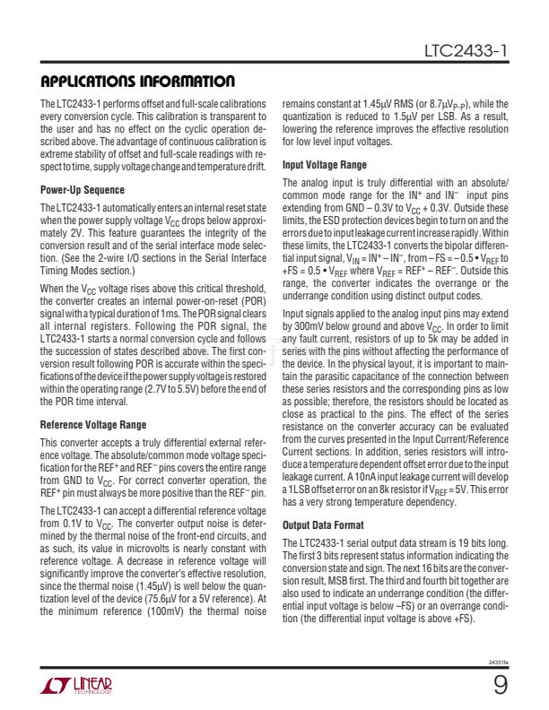
Table 3. LTC2433-1 State Duration
State
CONVERT
Operating Mode
Internal Oscillator
External Oscillator
F
O
= LOW
Simultaneous 50Hz/60Hz Rejection
F
O
= External Oscillator
with Frequency f
EOSC
kHz
(f
EOSC
/2560 Rejection)
F
O
= LOW
(Internal Oscillator)
F
O
= External Oscillator with
Frequency f
EOSC
kHz
SLEEP
DATA OUTPUT
Internal Serial Clock
External Serial Clock with
Frequency f
SCK
kHz
12
U
dividing the internal conversion clock by 8. In the External
SCK mode of operation, the SCK pin is used as input. The
internal or external SCK mode is selected on power-up and
then reselected every time a HIGH-to-LOW transition is
detected at the CS pin. If SCK is HIGH or floating at power-
up or during this transition, the converter enters the inter-
nal SCK mode. If SCK is LOW at power-up or during this
transition, the converter enters the external SCK mode.
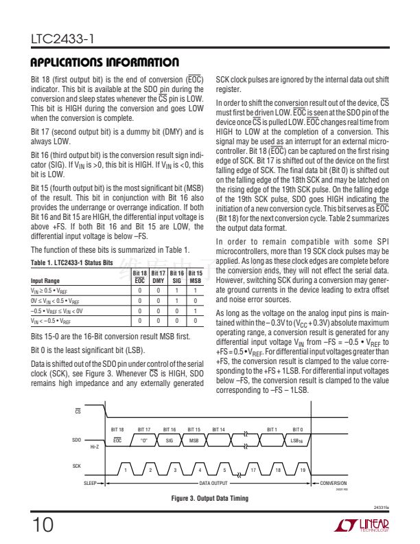
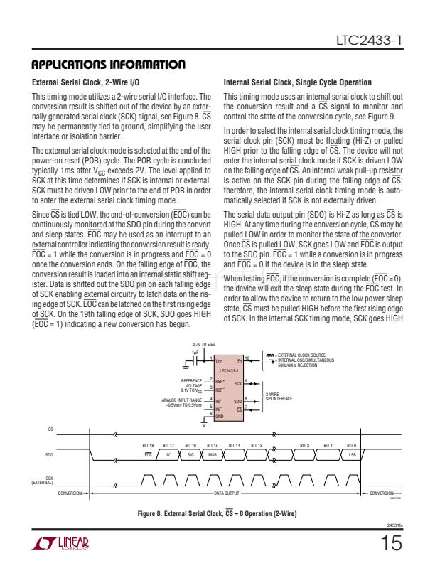
Serial Data Output (SDO)
The serial data output pin, SDO (Pin 8), provides the result
of the last conversion as a serial bit stream (MSB first)
during the data output state. In addition, the SDO pin is
used as an end of conversion indicator during the conver-
sion and sleep states.
When CS (Pin 7) is HIGH, the SDO driver is switched to a
high impedance state. This allows sharing the serial
interface with other devices. If CS is LOW during the
convert or sleep state, SDO will output EOC. If CS is LOW
during the conversion phase, the EOC bit appears HIGH on
the SDO pin. Once the conversion is complete, EOC goes
LOW.
Chip Select Input (CS)
The active LOW chip select, CS (Pin 7), is used to test the
conversion status and to enable the data output transfer as
described in the previous sections.
Duration
147ms, Output Data Rate
鈮?/div>
6.8 Readings/s
20510/f
EOSC
s, Output Data Rate
鈮?/div>
f
EOSC
/20510 Readings/s
As Long As CS = HIGH Until CS = LOW and SCK
As Long As CS = LOW But Not Longer Than 1.09ms
(19 SCK cycles)
As Long As CS = LOW But Not Longer Than 152/f
EOSC
ms
(19 SCK cycles)
As Long As CS = LOW But Not Longer Than 19/f
SCK
ms
(19 SCK cycles)
24331fa
W
U U


 1
1
 2
2
 3
3
 4
4
 5
5
 6
6
 7
7
 8
8
 9
9
 10
10
 11
11
 12
12
 13
13
 14
14
 15
15
 16
16
 17
17
 18
18
 19
19
 20
20
 21
21
 22
22
 23
23
 24
24
 25
25
 26
26
 27
27
 28
28
