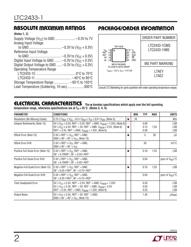
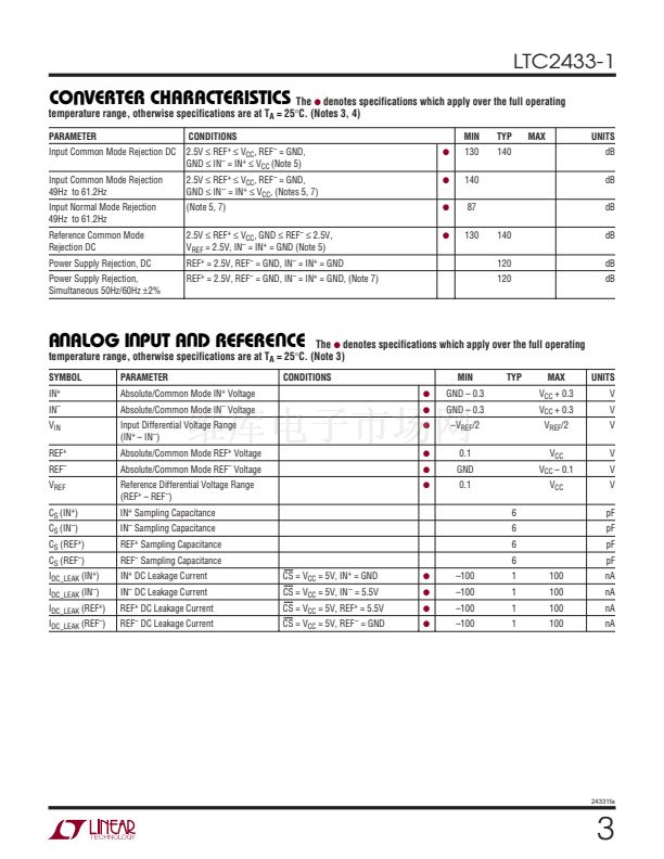
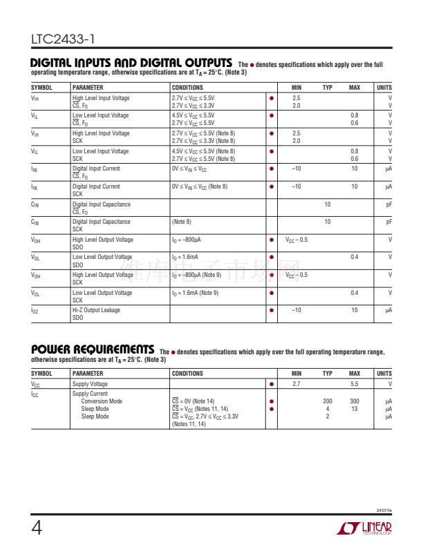
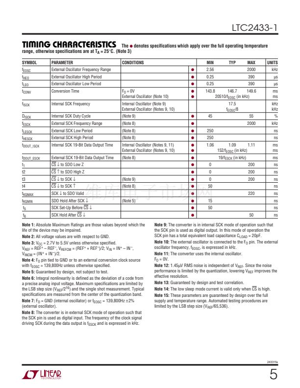
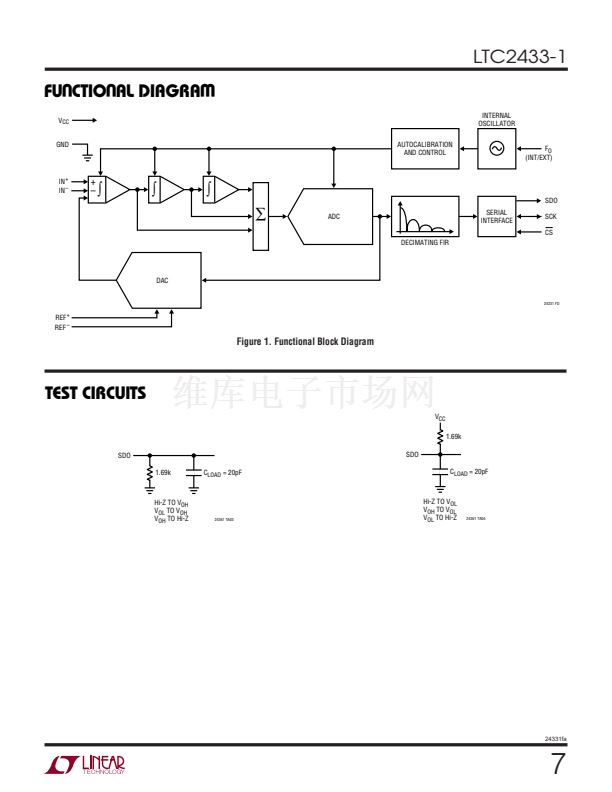
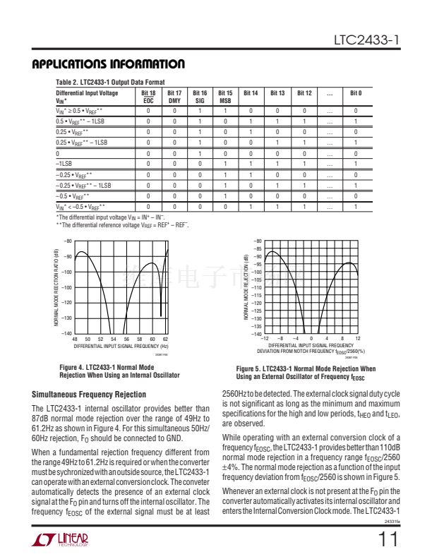
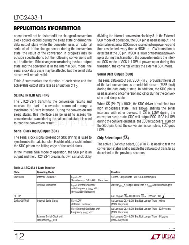
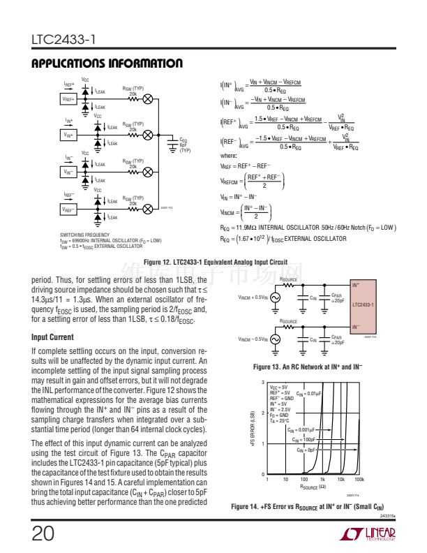
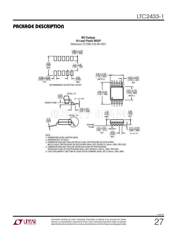
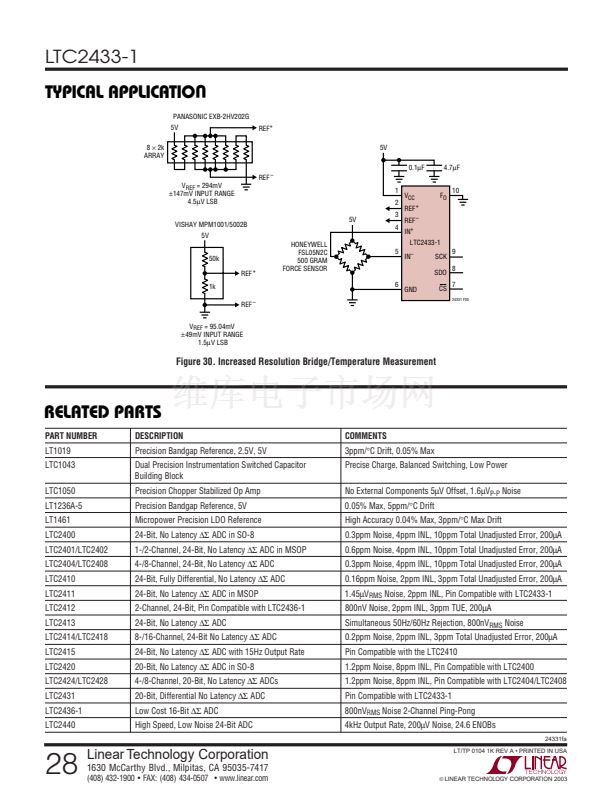
LTC2433-1
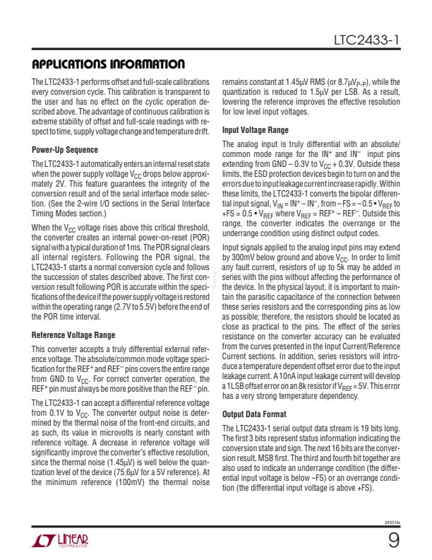
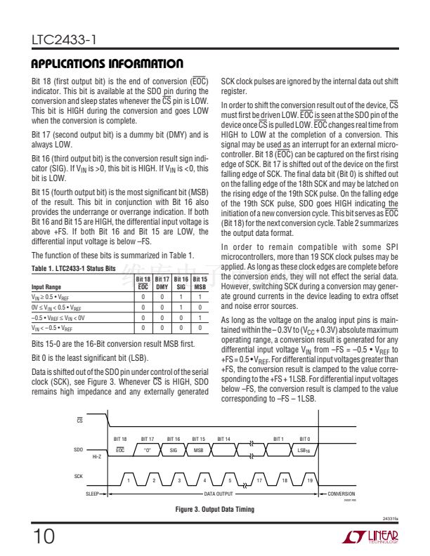
APPLICATIO S I FOR ATIO
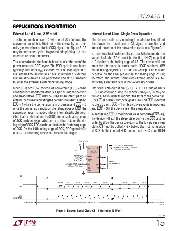
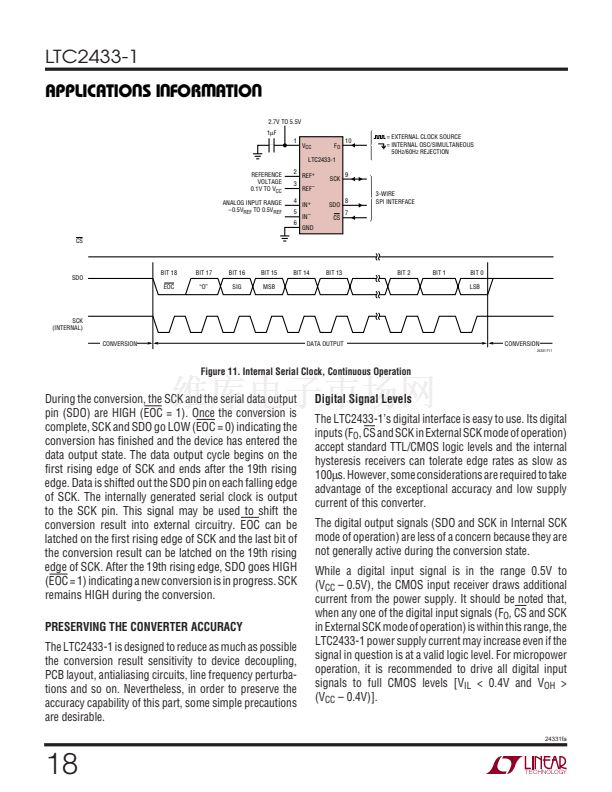
External Serial Clock, 2-Wire I/O
This timing mode utilizes a 2-wire serial I/O interface. The
conversion result is shifted out of the device by an exter-
nally generated serial clock (SCK) signal, see Figure 8. CS
may be permanently tied to ground, simplifying the user
interface or isolation barrier.
The external serial clock mode is selected at the end of the
power-on reset (POR) cycle. The POR cycle is concluded
typically 1ms after V
CC
exceeds 2V. The level applied to
SCK at this time determines if SCK is internal or external.
SCK must be driven LOW prior to the end of POR in order
to enter the external serial clock timing mode.
Since CS is tied LOW, the end-of-conversion (EOC) can be
continuously monitored at the SDO pin during the convert
and sleep states. EOC may be used as an interrupt to an
external controller indicating the conversion result is ready.
EOC = 1 while the conversion is in progress and EOC = 0
once the conversion ends. On the falling edge of EOC, the
conversion result is loaded into an internal static shift reg-
ister. Data is shifted out the SDO pin on each falling edge
of SCK enabling external circuitry to latch data on the ris-
ing edge of SCK. EOC can be latched on the first rising edge
of SCK. On the 19th falling edge of SCK, SDO goes HIGH
(EOC = 1) indicating a new conversion has begun.
2.7V TO 5.5V
1碌F
1
V
CC
ANALOG INPUT RANGE
鈥?.5V
REF
TO 0.5V
REF
CS
BIT 18
SDO
EOC
BIT 17
鈥淥鈥?/div>
SCK
(EXTERNAL)
CONVERSION
DATA OUTPUT
CONVERSION
24331 F08
Figure 8. External Serial Clock, CS = 0 Operation (2-Wire)
24331fa
U
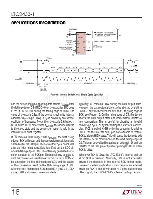
Internal Serial Clock, Single Cycle Operation
This timing mode uses an internal serial clock to shift out
the conversion result and a CS signal to monitor and
control the state of the conversion cycle, see Figure 9.
In order to select the internal serial clock timing mode, the
serial clock pin (SCK) must be floating (Hi-Z) or pulled
HIGH prior to the falling edge of CS. The device will not
enter the internal serial clock mode if SCK is driven LOW
on the falling edge of CS. An internal weak pull-up resistor
is active on the SCK pin during the falling edge of CS;
therefore, the internal serial clock timing mode is auto-
matically selected if SCK is not externally driven.
The serial data output pin (SDO) is Hi-Z as long as CS is
HIGH. At any time during the conversion cycle, CS may be
pulled LOW in order to monitor the state of the converter.
Once CS is pulled LOW, SCK goes LOW and EOC is output
to the SDO pin. EOC = 1 while a conversion is in progress
and EOC = 0 if the device is in the sleep state.
When testing EOC, if the conversion is complete (EOC = 0),
the device will exit the sleep state during the EOC test. In
order to allow the device to return to the low power sleep
state, CS must be pulled HIGH before the first rising edge
of SCK. In the internal SCK timing mode, SCK goes HIGH
F
O
10
= EXTERNAL CLOCK SOURCE
= INTERNAL OSC/SIMULTANEOUS
50Hz/60Hz REJECTION
LTC2433-1
REFERENCE
VOLTAGE
0.1V TO V
CC
2
3
4
5
6
REF
+
REF
鈥?/div>
IN
+
IN
鈥?/div>
GND
SDO
CS
8
7
SCK
9
3-WIRE
SPI INTERFACE
BIT 16
SIG
BIT 15
MSB
BIT 14
BIT 13
BIT 2
BIT 1
BIT 0
LSB
W
U U
15


 1
1
 2
2
 3
3
 4
4
 5
5
 6
6
 7
7
 8
8
 9
9
 10
10
 11
11
 12
12
 13
13
 14
14
 15
15
 16
16
 17
17
 18
18
 19
19
 20
20
 21
21
 22
22
 23
23
 24
24
 25
25
 26
26
 27
27
 28
28
