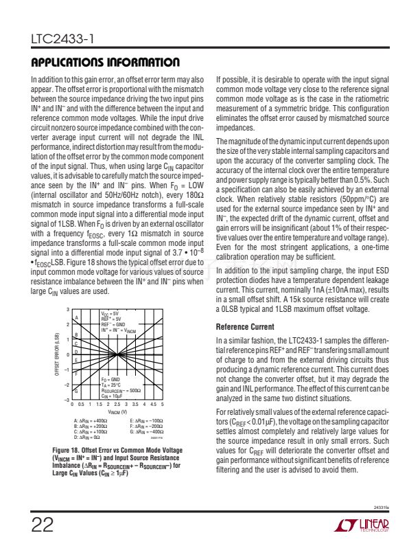
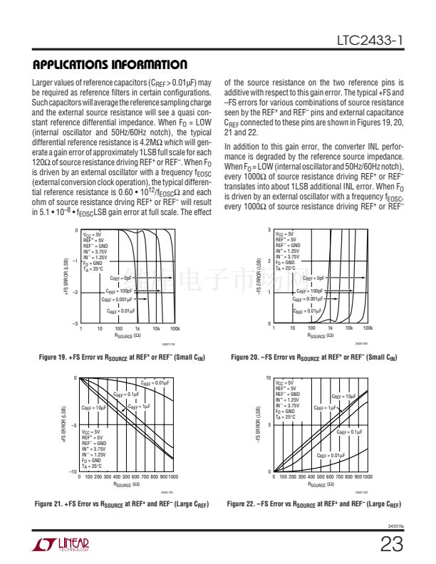
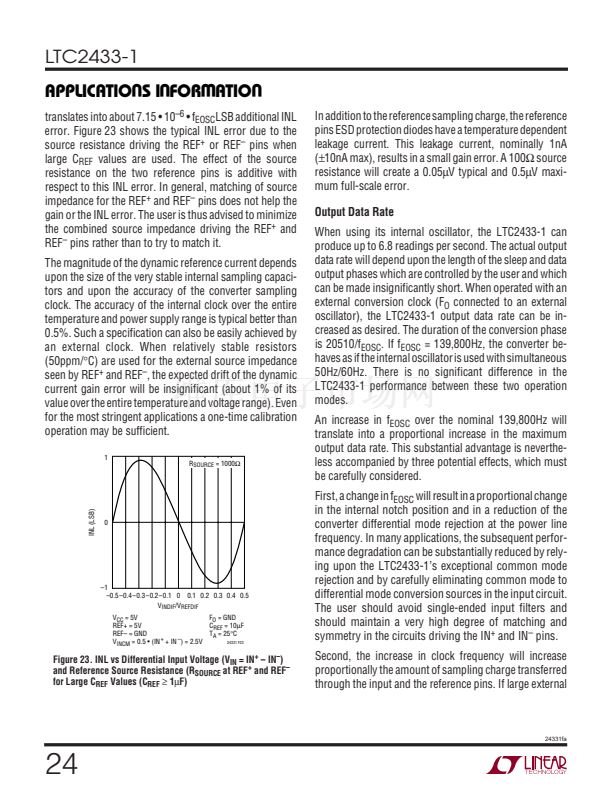
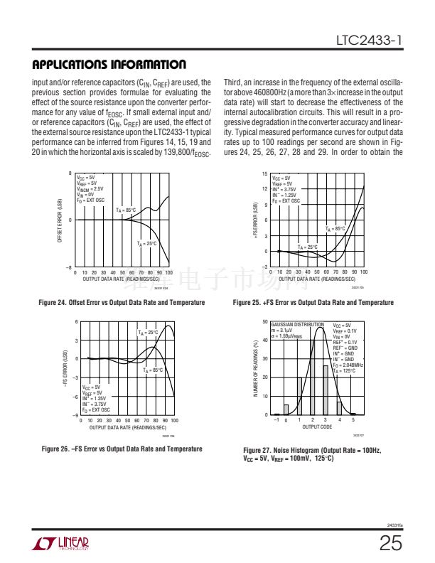
LTAEZ Datasheet

  • LTAEZ

  • Linear Integrated Systems [Differential Input 16-Bit No Lat...

  • 306.93KB

  • LINEAR

扫码查看芯片数据手册

上传产品规格书

PDF预览

LTC2433-1
APPLICATIO S I FOR ATIO
ANALOG INPUT RANGE
鈥?.5V
REF
TO 0.5V
REF
<t
EOCtest
CS
TEST EOC
BIT 18
SDO
Hi-Z
Hi-Z
EOC
BIT 17
鈥淥鈥?/div>
SCK
(INTERNAL)
CONVERSION
SLEEP
SLEEP
DATA OUTPUT
CONVERSION
24331 F09
TEST EOC
(OPTIONAL)
Figure 9. Internal Serial Clock, Single Cycle Operation
and the device begins outputting data at time t
EOCtest
after
the falling edge of CS (if EOC = 0) or t
EOCtest
after EOC goes
LOW (if CS is LOW during the falling edge of EOC). The
value of t
EOCtest
is 23碌s if the device is using its internal
oscillator (F
0
= logic LOW). If F
O
is driven by an external
oscillator of frequency f
EOSC
, then t
EOCtest
is 3.6/f
EOSC
. If
CS is pulled HIGH before time t
EOCtest
, the device returns
to the sleep state and the conversion result is held in the
internal static shift register.
If CS remains LOW longer than t
EOCtest
, the first rising
edge of SCK will occur and the conversion result is serially
shifted out of the SDO pin. The data output cycle concludes
after the 19th rising edge. Data is shifted out the SDO pin
on each falling edge of SCK. The internally generated serial
clock is output to the SCK pin. This signal may be used to
shift the conversion result into external circuitry. EOC can
be latched on the first rising edge of SCK and the last bit
of the conversion result on the 19th rising edge of SCK.
After the 19th rising edge, SDO goes HIGH (EOC = 1), SCK
stays HIGH and a new conversion starts.
16
U
2.7V TO 5.5V
1碌F
1
V
CC
F
O
10
= EXTERNAL CLOCK SOURCE
= INTERNAL OSC/SIMULTANEOUS
50Hz/60Hz REJECTION
V
CC
10k
LTC2433-1
REFERENCE
VOLTAGE
0.1V TO V
CC
2
3
4
5
6
REF
+
REF
鈥?/div>
IN
+
IN
鈥?/div>
GND
SDO
CS
8
7
SCK
9
3-WIRE
SPI INTERFACE
BIT 16
SIG
BIT 15
MSB
BIT 14
BIT 13
BIT 2
BIT 1
BIT 0
LSB
Hi-Z
Hi-Z
W
U U
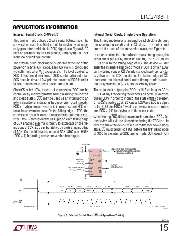
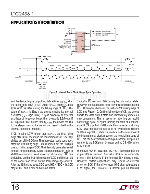
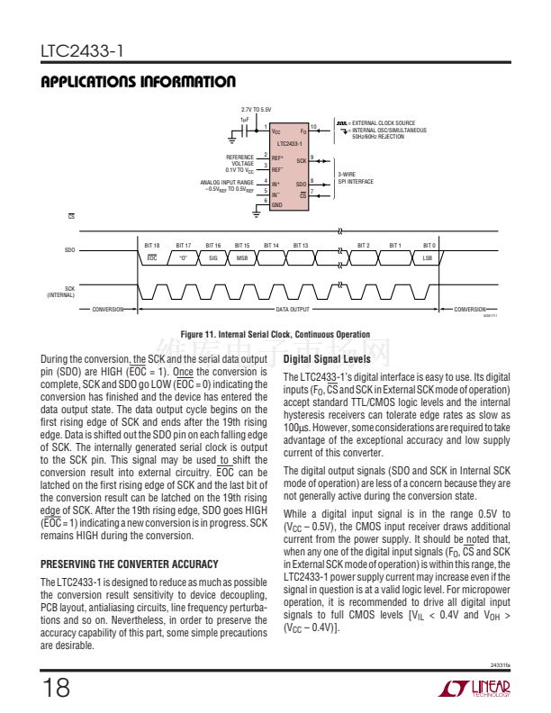
Typically, CS remains LOW during the data output state.
However, the data output state may be aborted by pulling
CS HIGH anytime between the first and 19th rising edge of
SCK, see Figure 10. On the rising edge of CS, the device
aborts the data output state and immediately initiates a
new conversion. This is useful for aborting an invalid
conversion cycle, or synchronizing the start of a conver-
sion. If CS is pulled HIGH while the converter is driving
SCK LOW, the internal pull-up is not available to restore
SCK to a logic HIGH state. This will cause the device to exit
the internal serial clock mode on the next falling edge of
CS. This can be avoided by adding an external 10k pull-up
resistor to the SCK pin or by never pulling CS HIGH when
SCK is LOW.
Whenever SCK is LOW, the LTC2433-1鈥檚 internal pull-up
at pin SCK is disabled. Normally, SCK is not externally
driven if the device is in the internal SCK timing mode.
However, certain applications may require an external
driver on SCK. If this driver goes Hi-Z after outputting a
LOW signal, the LTC2433-1鈥檚 internal pull-up remains
24331fa

LTAEZ相关型号PDF文件下载

  • 型号
    版本
    描述
    厂商
    下载
  • 英文版
    Differential Input 16-Bit No Latency DS ADC
    LINEAR
  • 英文版
    Linear Integrated Systems [Differential Input 16-Bit No Lat...
    LINEAR

您可能感兴趣的PDF文件资料

扫码下载APP,
一键连接广大的电子世界。

在线人工客服

买家服务:
卖家服务:

0571-85317607

客服在线时间周一至周五
9:00-17:30

关注官方微信号,
第一时间获取资讯。

建议反馈

联系人:

联系方式:

按住滑块,拖拽到最右边
>>
感谢您向阿库提出的宝贵意见,您的参与是维库提升服务的动力!意见一经采纳,将有感恩红包奉上哦!