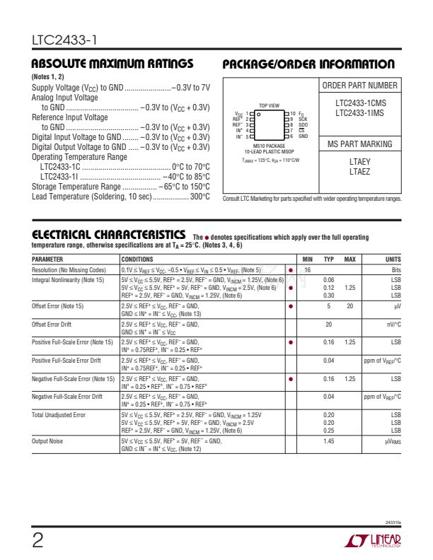
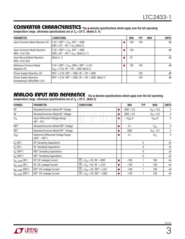
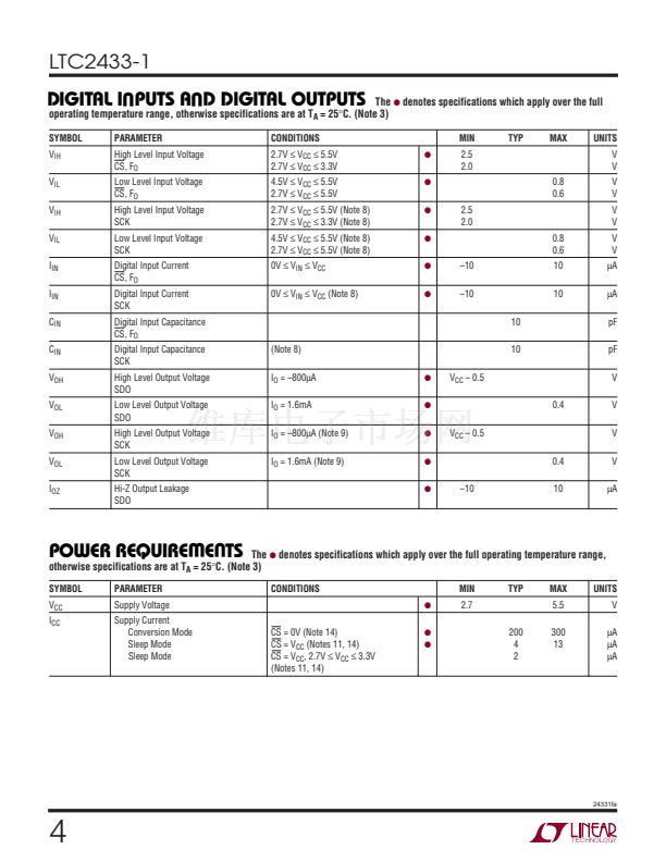
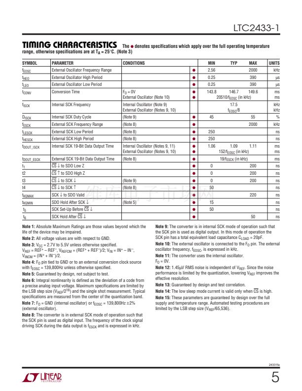
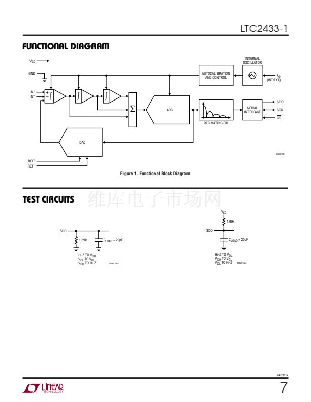
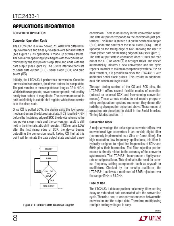
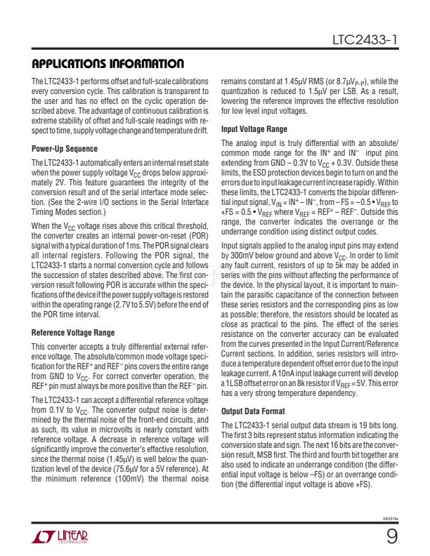
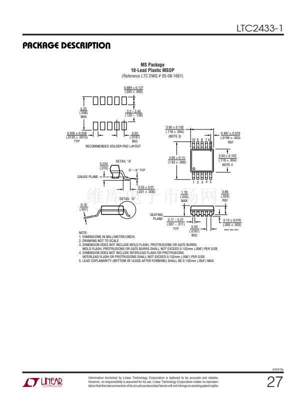
LTC2433-1
APPLICATIO S I FOR ATIO
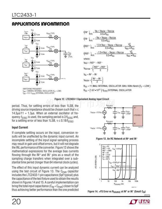
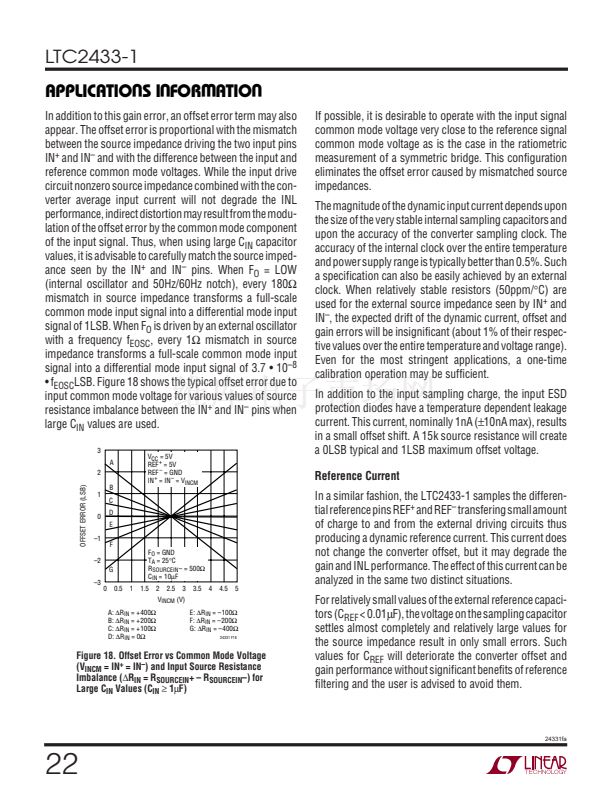
ANALOG INPUT RANGE
鈥?.5V
REF
TO 0.5V
REF
> t
EOCtest
CS
TEST EOC
<t
EOCtest
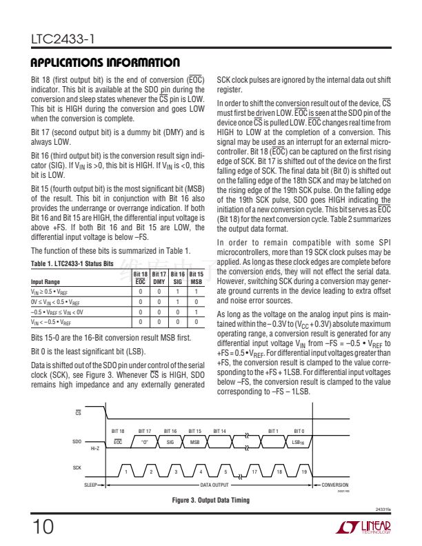
BIT 0
SDO
Hi-Z
EOC
Hi-Z
Hi-Z
Hi-Z
SCK
(INTERNAL)
SLEEP
DATA
OUTPUT
CONVERSION
SLEEP
SLEEP
DATA OUTPUT
CONVERSION
24331 F10
TEST EOC
(OPTIONAL)
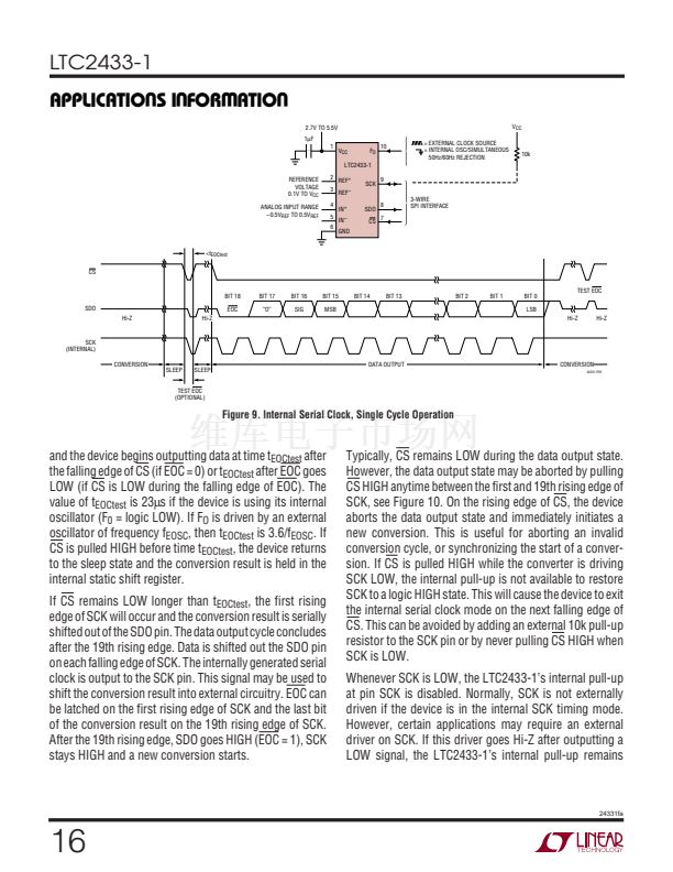
Figure 10. Internal Serial Clock, Reduced Data Output Length
disabled. Hence, SCK remains LOW. On the next falling
edge of CS, the device is switched to the external SCK
timing mode. By adding an external 10k pull-up resistor to
SCK, this pin goes HIGH once the external driver goes
Hi-Z. On the next CS falling edge, the device will remain in
the internal SCK timing mode.
A similar situation may occur during the sleep state when
CS is pulsed HIGH-LOW-HIGH in order to test the
conversion status. If the device is in the sleep state (EOC
= 0), SCK will go LOW. Once CS goes HIGH (within the time
period defined above as t
EOCtest
), the internal pull-up is
activated. For a heavy capacitive load on the SCK pin, the
internal pull-up may not be adequate to return SCK to a
HIGH level before CS goes low again. This is not a concern
under normal conditions where CS remains LOW after
detecting EOC = 0. This situation is easily overcome by
adding an external 10k pull-up resistor to the SCK pin.
U
2.7V TO 5.5V
1碌F
1
V
CC
F
O
10
= EXTERNAL CLOCK SOURCE
= INTERNAL OSC/SIMULTANEOUS
50Hz/60Hz REJECTION
V
CC
10k
LTC2433-1
REFERENCE
VOLTAGE
0.1V TO V
CC
2
3
4
5
6
REF
+
REF
鈥?/div>
IN
+
W
U U
SCK
9
3-WIRE
SPI INTERFACE
SDO
CS
8
7
IN
鈥?/div>
GND
BIT 18
EOC
BIT 17
鈥淥鈥?/div>
BIT 16
SIG
BIT 15
MSB
BIT 14
BIT 13
BIT 2
TEST EOC
Hi-Z
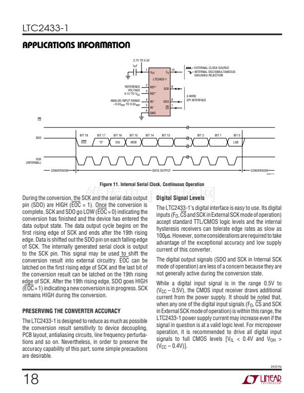
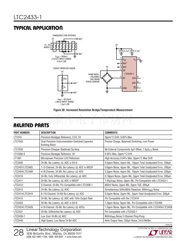
Internal Serial Clock, 2-Wire I/O,
Continuous Conversion
This timing mode uses a 2-wire, all output (SCK and SDO)
interface. The conversion result is shifted out of the device
by an internally generated serial clock (SCK) signal, see
Figure 11. CS may be permanently tied to ground, simpli-
fying the user interface or isolation barrier.
The internal serial clock mode is selected at the end of the
power-on reset (POR) cycle. The POR cycle is concluded
approximately 1ms after V
CC
exceeds 2V. An internal weak
pull-up is active during the POR cycle; therefore, the
internal serial clock timing mode is automatically selected
if SCK is not externally driven LOW (if SCK is loaded such
that the internal pull-up cannot pull the pin HIGH, the
external SCK mode will be selected).
24331fa
17


 1
1
 2
2
 3
3
 4
4
 5
5
 6
6
 7
7
 8
8
 9
9
 10
10
 11
11
 12
12
 13
13
 14
14
 15
15
 16
16
 17
17
 18
18
 19
19
 20
20
 21
21
 22
22
 23
23
 24
24
 25
25
 26
26
 27
27
 28
28
