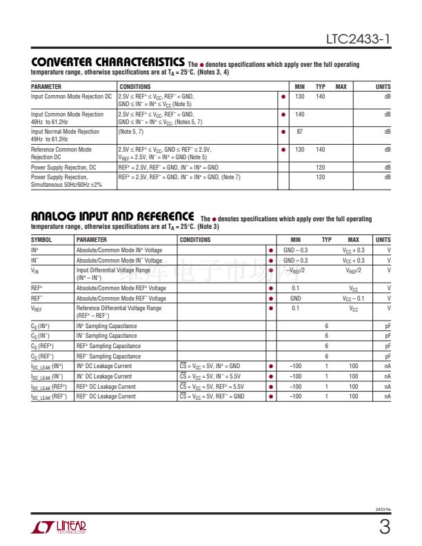
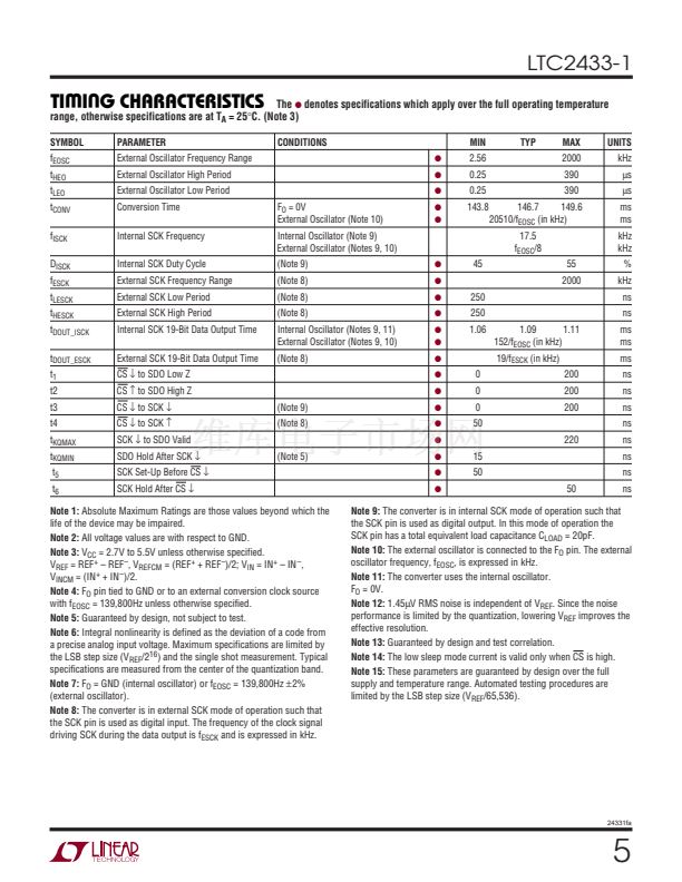
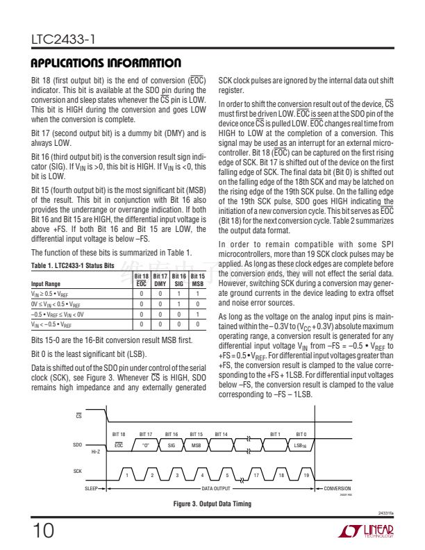
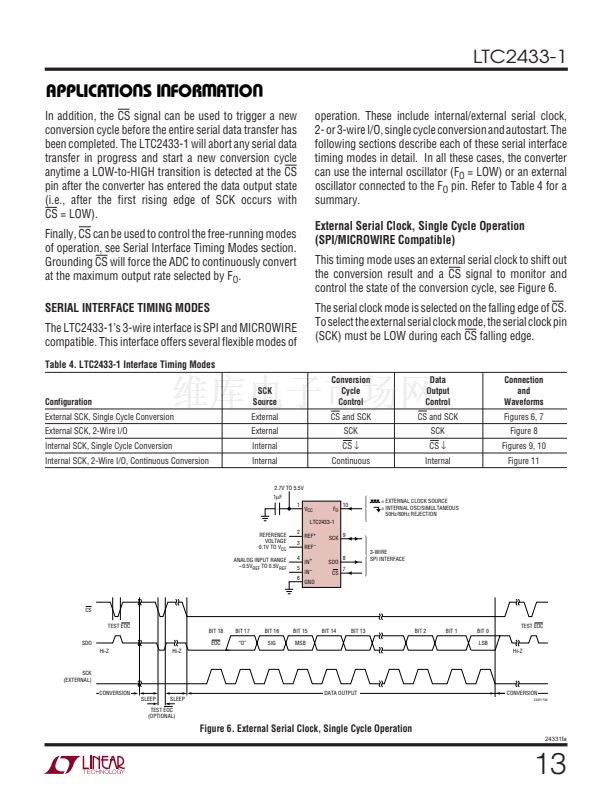
鈥淥鈥?/div>
BIT 16
SIG
SCK
(INTERNAL)
CONVERSION
DATA OUTPUT
CONVERSION
24331 F11
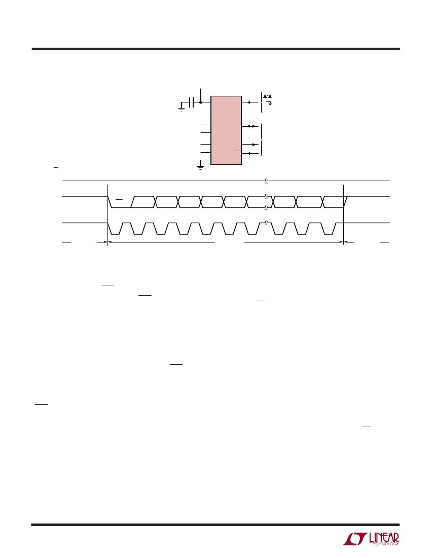
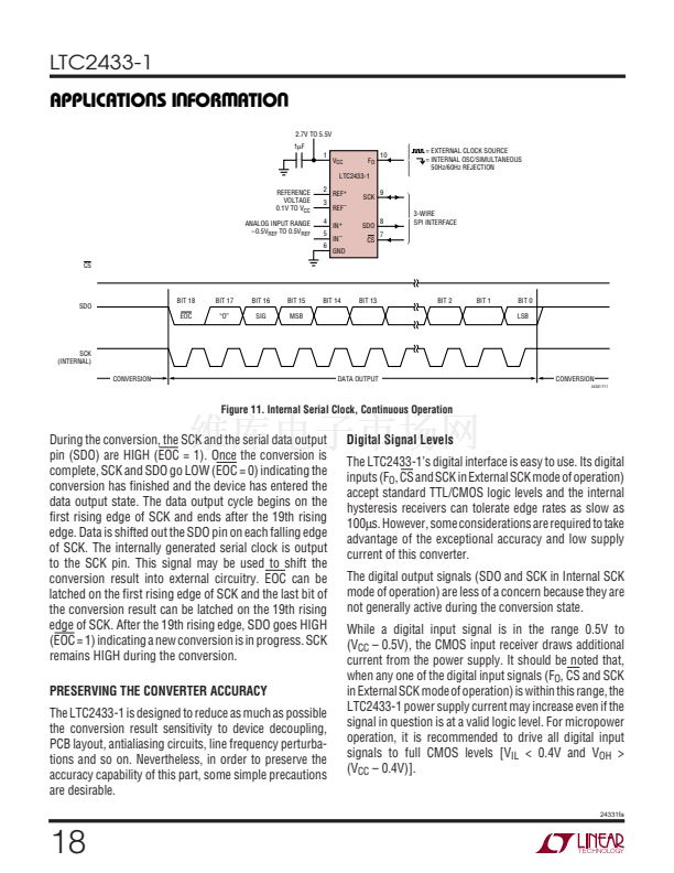
Figure 11. Internal Serial Clock, Continuous Operation
During the conversion, the SCK and the serial data output
pin (SDO) are HIGH (EOC = 1). Once the conversion is
complete, SCK and SDO go LOW (EOC = 0) indicating the
conversion has finished and the device has entered the
data output state. The data output cycle begins on the
first rising edge of SCK and ends after the 19th rising
edge. Data is shifted out the SDO pin on each falling edge
of SCK. The internally generated serial clock is output
to the SCK pin. This signal may be used to shift the
conversion result into external circuitry. EOC can be
latched on the first rising edge of SCK and the last bit of
the conversion result can be latched on the 19th rising
edge of SCK. After the 19th rising edge, SDO goes HIGH
(EOC = 1) indicating a new conversion is in progress. SCK
remains HIGH during the conversion.
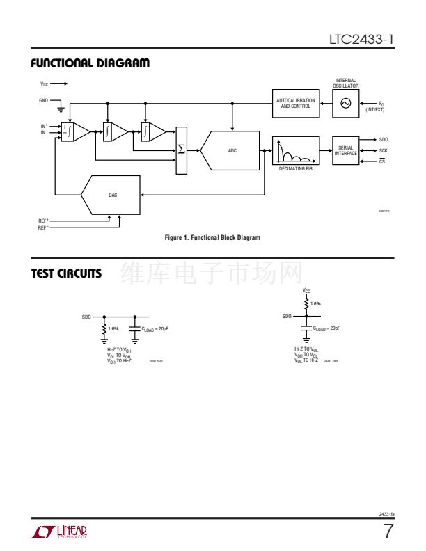
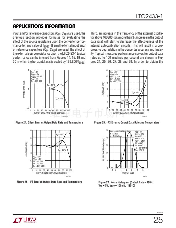
PRESERVING THE CONVERTER ACCURACY
The LTC2433-1 is designed to reduce as much as possible
the conversion result sensitivity to device decoupling,
PCB layout, antialiasing circuits, line frequency perturba-
tions and so on. Nevertheless, in order to preserve the
accuracy capability of this part, some simple precautions
are desirable.
18
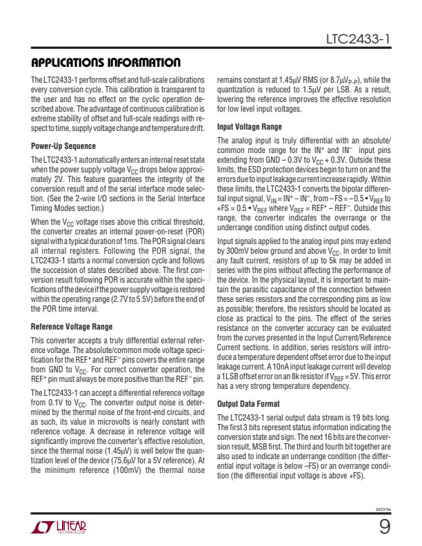
U
2.7V TO 5.5V
1碌F
1
V
CC
F
O
10
= EXTERNAL CLOCK SOURCE
= INTERNAL OSC/SIMULTANEOUS
50Hz/60Hz REJECTION
LTC2433-1
2
3
4
5
6
REF
+
REF
鈥?/div>
IN
+
IN
鈥?/div>
GND
SDO
CS
8
7
SCK
9
3-WIRE
SPI INTERFACE
BIT 15
MSB
BIT 14
BIT 13
BIT 2
BIT 1
BIT 0
LSB
W
U U
Digital Signal Levels
The LTC2433-1鈥檚 digital interface is easy to use. Its digital
inputs (F
O
, CS and SCK in External SCK mode of operation)
accept standard TTL/CMOS logic levels and the internal
hysteresis receivers can tolerate edge rates as slow as
100碌s. However, some considerations are required to take
advantage of the exceptional accuracy and low supply
current of this converter.
The digital output signals (SDO and SCK in Internal SCK
mode of operation) are less of a concern because they are
not generally active during the conversion state.
While a digital input signal is in the range 0.5V to
(V
CC
鈥?0.5V), the CMOS input receiver draws additional
current from the power supply. It should be noted that,
when any one of the digital input signals (F
O
, CS and SCK
in External SCK mode of operation) is within this range, the
LTC2433-1 power supply current may increase even if the
signal in question is at a valid logic level. For micropower
operation, it is recommended to drive all digital input
signals to full CMOS levels [V
IL
< 0.4V and V
OH
>
(V
CC
鈥?0.4V)].
24331fa


 1
1
 2
2
 3
3
 4
4
 5
5
 6
6
 7
7
 8
8
 9
9
 10
10
 11
11
 12
12
 13
13
 14
14
 15
15
 16
16
 17
17
 18
18
 19
19
 20
20
 21
21
 22
22
 23
23
 24
24
 25
25
 26
26
 27
27
 28
28
