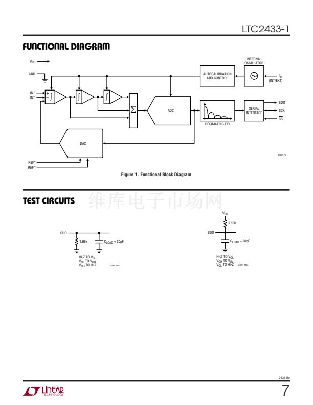
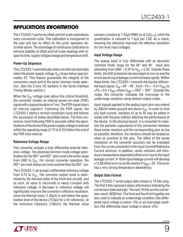
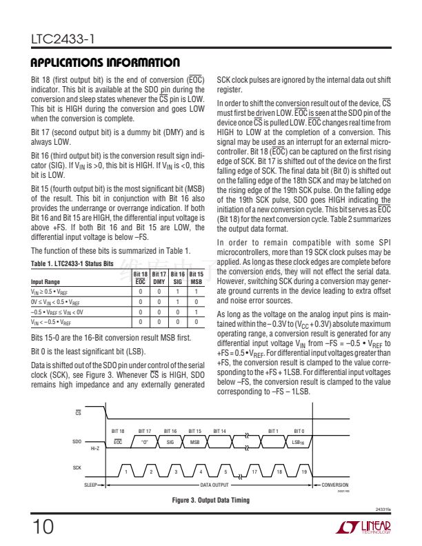
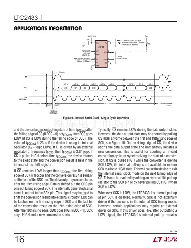
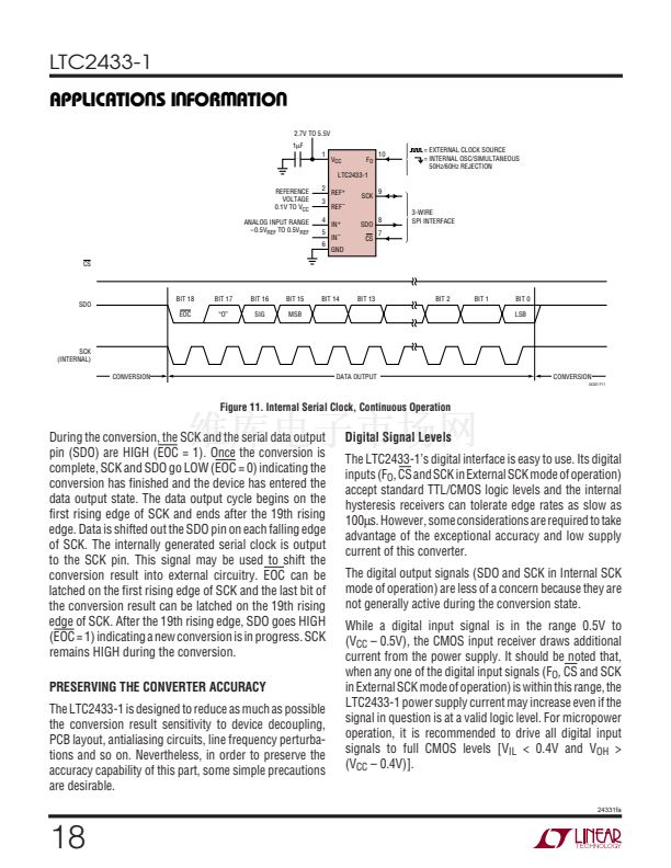
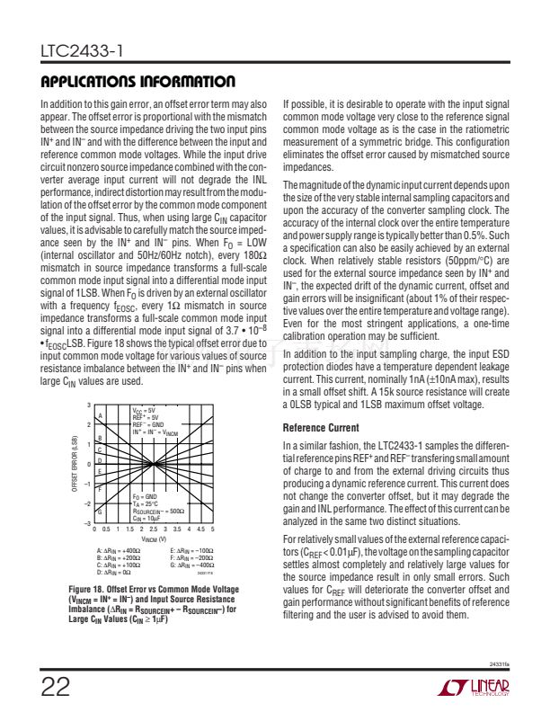
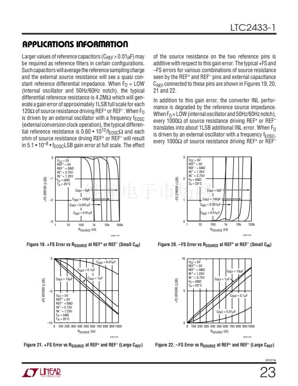
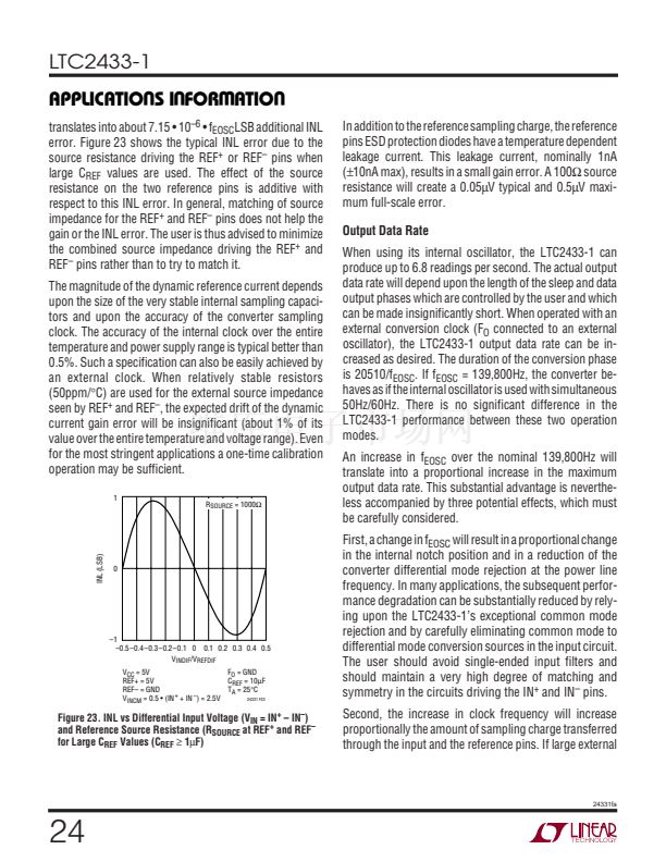
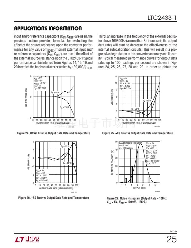
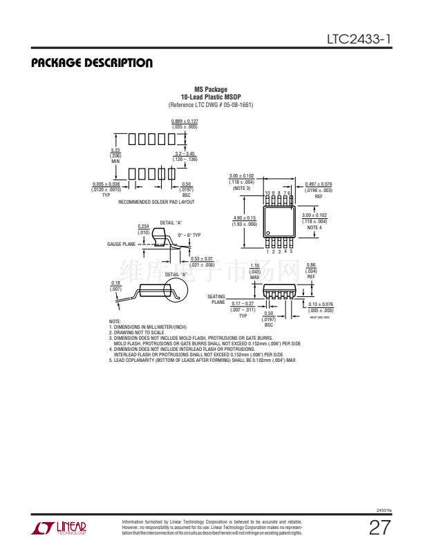
LTC2433-1
APPLICATIO S I FOR ATIO
During the conversion period, the undershoot and/or
overshoot of a fast digital signal connected to the
LTC2433-1 pins may severely disturb the analog to digital
conversion process. Undershoot and overshoot can oc-
cur because of the impedance mismatch at the converter
pin when the transition time of an external control signal
is less than twice the propagation delay from the driver to
LTC2433-1. For reference, on a regular FR-4 board, signal
propagation velocity is approximately 183ps/inch for
internal traces and 170ps/inch for surface traces. Thus, a
driver generating a control signal with a minimum transi-
tion time of 1ns must be connected to the converter pin
through a trace shorter than 2.5 inches. This problem
becomes particularly difficult when shared control lines
are used and multiple reflections may occur. The solution
is to carefully terminate all transmission lines close to
their characteristic impedance.
Parallel termination near the LTC2433-1 pin will eliminate
this problem but will increase the driver power dissipation.
A series resistor between 27鈩?and 56鈩?placed near the
driver will also eliminate this problem without additional
power dissipation. The actual resistor value depends upon
the trace impedance and connection topology.
An alternate solution is to reduce the edge rate of the
control signals. It should be noted that using very slow
edges will increase the converter power supply current
during the transition time. The multiple ground pins used
in this package configuration, as well as the differential
input and reference architecture, reduce substantially the
converter鈥檚 sensitivity to ground currents.
Particular attention must be given to the connection of the
F
O
signal when the LTC2433-1 is used with an external
conversion clock. This clock is active during the conver-
sion time and the normal mode rejection provided by the
internal digital filter is not very high at this frequency. A
normal mode signal of this frequency at the converter
reference terminals may result in DC gain and INL errors.
A normal mode signal of this frequency at the converter
input terminals may result in a DC offset error. Such
U
perturbations may occur due to asymmetric capacitive
coupling between the F
O
signal trace and the converter
input and/or reference connection traces. An immediate
solution is to maintain maximum possible separation
between the F
O
signal trace and the input/reference sig-
nals. When the F
O
signal is parallel terminated near the
converter, substantial AC current is flowing in the loop
formed by the F
O
connection trace, the termination and the
ground return path. Thus, perturbation signals may be
inductively coupled into the converter input and/or refer-
ence. In this situation, the user must reduce to a minimum
the loop area for the F
O
signal as well as the loop area for
the differential input and reference connections.
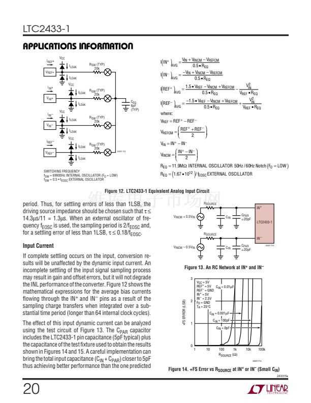
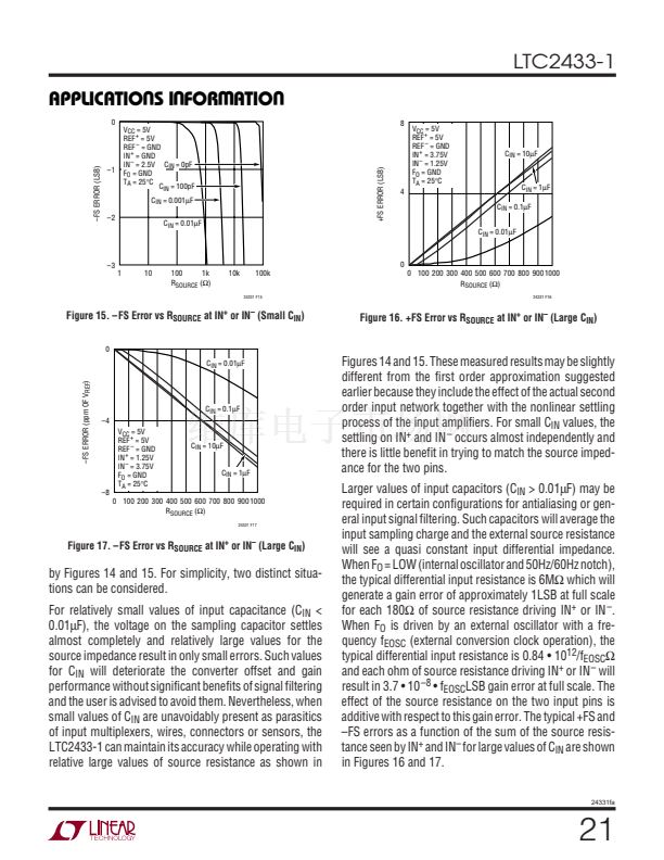
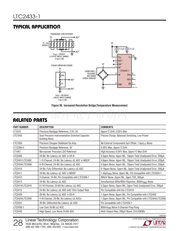
Driving the Input and Reference
The input and reference pins of the LTC2433-1 converter
are directly connected to a network of sampling capaci-
tors. Depending upon the relation between the differential
input voltage and the differential reference voltage, these
capacitors are switching between these four pins
transfering small amounts of charge in the process. A
simplified equivalent circuit is shown in Figure 12, where
IN
+
and IN
鈥?/div>
refer to the selected differential channel and
the unselected channel is omitted for simplicity.
For a simple approximation, the source impedance R
S
driving an analog input pin (IN
+
, IN
鈥?/div>
, REF
+
or REF
鈥?/div>
) can be
considered to form, together with R
SW
and C
EQ
(see
Figure 12), a first order passive network with a time
constant
蟿
= (R
S
+ R
SW
) 鈥?C
EQ
. The converter is able to
sample the input signal with better than 1LSB accuracy if
the sampling period is at least 11 times greater than the
input circuit time constant
蟿.
The sampling process on the
four input analog pins is quasi-independent so each time
constant should be considered by itself and, under worst-
case circumstances, the errors may add.
When using the internal oscillator (F
O
= LOW), the
LTC2433-1鈥檚 front-end switched-capacitor network is
clocked at 69900Hz corresponding to a 14.3碌s sampling
24331fa
W
U U
19


 1
1
 2
2
 3
3
 4
4
 5
5
 6
6
 7
7
 8
8
 9
9
 10
10
 11
11
 12
12
 13
13
 14
14
 15
15
 16
16
 17
17
 18
18
 19
19
 20
20
 21
21
 22
22
 23
23
 24
24
 25
25
 26
26
 27
27
 28
28
