LTAEZ Datasheet

  • LTAEZ

  • Linear Integrated Systems [Differential Input 16-Bit No Lat...

  • 306.93KB

  • LINEAR

扫码查看芯片数据手册

上传产品规格书

PDF预览

LTC2433-1
APPLICATIO S I FOR ATIO
The LTC2433-1 performs offset and full-scale calibrations
every conversion cycle. This calibration is transparent to
the user and has no effect on the cyclic operation de-
scribed above. The advantage of continuous calibration is
extreme stability of offset and full-scale readings with re-
spect to time, supply voltage change and temperature drift.
Power-Up Sequence
The LTC2433-1 automatically enters an internal reset state
when the power supply voltage V
CC
drops below approxi-
mately 2V. This feature guarantees the integrity of the
conversion result and of the serial interface mode selec-
tion. (See the 2-wire I/O sections in the Serial Interface
Timing Modes section.)
When the V
CC
voltage rises above this critical threshold,
the converter creates an internal power-on-reset (POR)
signal with a typical duration of 1ms. The POR signal clears
all internal registers. Following the POR signal, the
LTC2433-1 starts a normal conversion cycle and follows
the succession of states described above. The first con-
version result following POR is accurate within the speci-
fications of the device if the power supply voltage is restored
within the operating range (2.7V to 5.5V) before the end of
the POR time interval.
Reference Voltage Range
This converter accepts a truly differential external refer-
ence voltage. The absolute/common mode voltage speci-
fication for the REF
+
and REF
鈥?/div>
pins covers the entire range
from GND to V
CC
. For correct converter operation, the
REF
+
pin must always be more positive than the REF
鈥?/div>
pin.
The LTC2433-1 can accept a differential reference voltage
from 0.1V to V
CC
. The converter output noise is deter-
mined by the thermal noise of the front-end circuits, and
as such, its value in microvolts is nearly constant with
reference voltage. A decrease in reference voltage will
significantly improve the converter鈥檚 effective resolution,
since the thermal noise (1.45碌V) is well below the quan-
tization level of the device (75.6碌V for a 5V reference). At
the minimum reference (100mV) the thermal noise
U
remains constant at 1.45碌V RMS (or 8.7碌V
P-P
), while the
quantization is reduced to 1.5碌V per LSB. As a result,
lowering the reference improves the effective resolution
for low level input voltages.
Input Voltage Range
The analog input is truly differential with an absolute/
common mode range for the IN
+
and IN
鈥?/div>
input pins
extending from GND 鈥?0.3V to V
CC
+ 0.3V. Outside these
limits, the ESD protection devices begin to turn on and the
errors due to input leakage current increase rapidly. Within
these limits, the LTC2433-1 converts the bipolar differen-
tial input signal, V
IN
= IN
+
鈥?IN
鈥?/div>
, from 鈥?FS = 鈥?0.5 鈥?V
REF
to
+FS = 0.5 鈥?V
REF
where V
REF
= REF
+
鈥?REF
鈥?/div>
. Outside this
range, the converter indicates the overrange or the
underrange condition using distinct output codes.
Input signals applied to the analog input pins may extend
by 300mV below ground and above V
CC
. In order to limit
any fault current, resistors of up to 5k may be added in
series with the pins without affecting the performance of
the device. In the physical layout, it is important to main-
tain the parasitic capacitance of the connection between
these series resistors and the corresponding pins as low
as possible; therefore, the resistors should be located as
close as practical to the pins. The effect of the series
resistance on the converter accuracy can be evaluated
from the curves presented in the Input Current/Reference
Current sections. In addition, series resistors will intro-
duce a temperature dependent offset error due to the input
leakage current. A 10nA input leakage current will develop
a 1LSB offset error on an 8k resistor if V
REF
= 5V. This error
has a very strong temperature dependency.
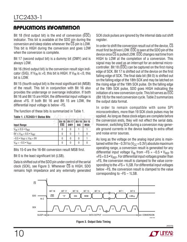
Output Data Format
The LTC2433-1 serial output data stream is 19 bits long.
The first 3 bits represent status information indicating the
conversion state and sign. The next 16 bits are the conver-
sion result, MSB first. The third and fourth bit together are
also used to indicate an underrange condition (the differ-
ential input voltage is below 鈥揊S) or an overrange condi-
tion (the differential input voltage is above +FS).
24331fa
W
U U
9

LTAEZ相关型号PDF文件下载

  • 型号
    版本
    描述
    厂商
    下载
  • 英文版
    Differential Input 16-Bit No Latency DS ADC
    LINEAR
  • 英文版
    Linear Integrated Systems [Differential Input 16-Bit No Lat...
    LINEAR

您可能感兴趣的PDF文件资料

扫码下载APP,
一键连接广大的电子世界。

在线人工客服

买家服务:
卖家服务:

0571-85317607

客服在线时间周一至周五
9:00-17:30

关注官方微信号,
第一时间获取资讯。

建议反馈

联系人:

联系方式:

按住滑块,拖拽到最右边
>>
感谢您向阿库提出的宝贵意见,您的参与是维库提升服务的动力!意见一经采纳,将有感恩红包奉上哦!