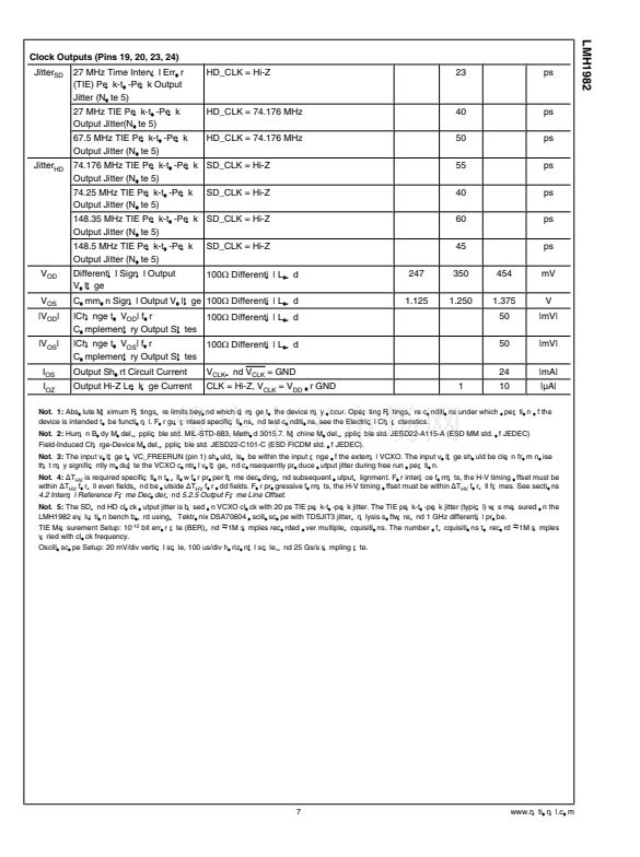
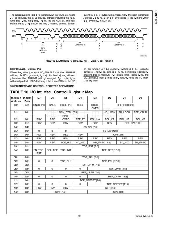
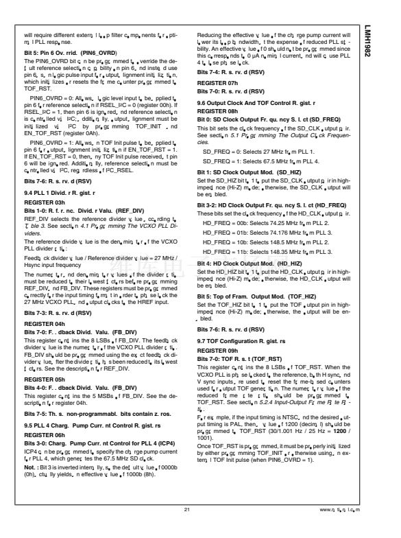
LMH1982
4.0 INPUT REFERENCE
The LMH1982 features two reference ports (A and B) with H
sync and V sync inputs which are used for phase locking the
outputs in Genlock mode. The reference port can be selected
by programming RSEL (register 00h). If desired, REF_SEL
input can be used instead to select the reference port by ini-
tially setting I
2
C_RSEL = 0 (register 00h).
The reference signals should be 3.3V LVCMOS signals within
the input voltage range specified in the Electrical Character-
istics table. The H sync and V sync input signals may have
analog timing, such as from the LMH1981 multi-format analog
video sync separator, or digital timing, such as from an FPGA
SDI deserializer.
4.1 Programming The VCXO PLL Dividers
To genlock the outputs to the reference, it is necessary to
phase lock the VCXO PLL clock to the H sync input signal by
programming its dividers. The PLL divider values are deter-
mined by the following ratio:
f
VCXO
/ f
HSYNC
= Feedback Divider / Reference Divider
Where:
f
VCXO
= 27 MHz VCXO frequency
f
HSYNC
= H sync input frequency
Feedback Divider = 1 to 8191
Reference Divider = 1, 2 or 5
The reference divider value can be selected from
Table 3
and
programmed to REF_DIV (register 03h). The feedback di-
vider value can be selected from
Table 4
and programmed to
FB_DIV (register 04h-05h).
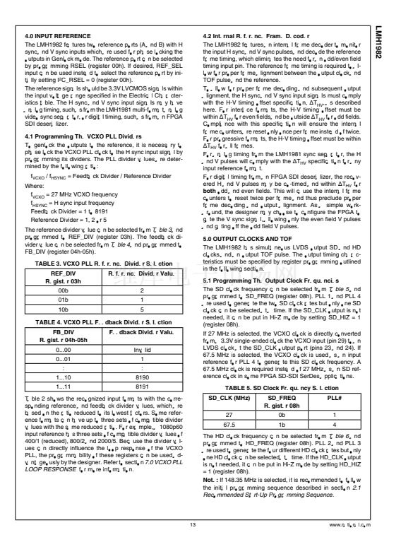
TABLE 3. VCXO PLL Reference Divider Selection
REF_DIV
Register 03h
00b
01b
10b
Reference Divider Value
2
1
5
4.2 Internal Reference Frame Decoder
The LMH1982 features an internal frame decoder to monitor
the input H sync and V sync pulses and decode the reference
frame timing, which eliminates the need for an odd/even field
timing input pin. The reference frame timing is required to al-
low for proper frame alignment between the output clock and
TOF pulse and the reference.
To allow for proper frame decoding and subsequent output
alignment, the H sync and V sync input signals must comply
with the H-V timing offset specification,
螖T
HV
, as described
here. For interlace formats, the H-V timing offset must be
within
螖T
HV
for even fields and be outside
螖T
HV
for odd fields.
Compliance with this specification will ensure the internal
frame counters are reset only once per frame instead of twice.
For progressive formats, the H-V timing offset must be within
螖T
HV
for all frames.
For analog timing from the LMH1981 sync separator, the H
and V pulses will comply with the
螖T
HV
specification for any
input reference format.
For digital timing from an FPGA SDI deserializer, the recov-
ered H and V pulses may be co-timed and within
螖T
HV
for
both
odd and even fields. This will cause the internal frame
counters to reset twice per frame and thus preclude proper
frame decoding and output alignment. As a simple work-
around, the designer may choose to configure the FPGA to
gate the V sync signal, allowing only the even field V pulses
and gating off the odd field V pulses.
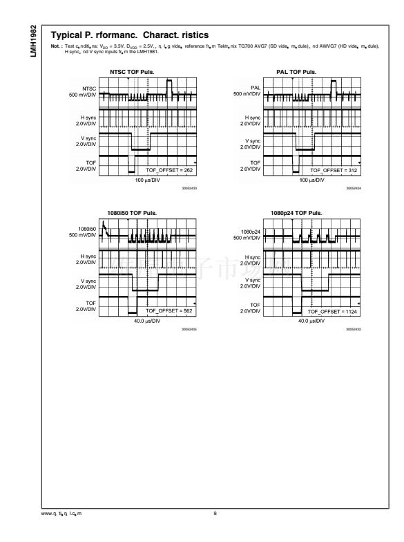
5.0 OUTPUT CLOCKS AND TOF
The LMH1982 has simultaneous LVDS output SD and HD
clocks and an output TOF pulse. The output timing charac-
teristics must be specified by register programming outlined
in the following section.
5.1 Programming The Output Clock Frequencies
The SD clock frequency can be selected from
Table 5
and
programmed to SD_FREQ (register 08h). PLL 1 and PLL 4
are used to generate the two SD clock rates but only one SD
clock can be selected at a time. If the SD_CLK output is not
needed, it can be put in Hi-Z mode by setting SD_HIZ = 1
(register 08h).
If 27 MHz is selected, the VCXO clock is directly converted
from a 3.3V single-ended clock the VCXO input (pin 29) to an
LVDS clock at the SD_CLK output port (pins 23 and 24). If
67.5 MHz is selected, the VCXO clock is used as an input
reference for PLL 4 to generate this SD clock frequency. A
67.5 MHz clock is required instead of 27 MHz as an SD ref-
erence clock in some FPGA SD-SDI SerDes applications.
TABLE 5. SD Clock Frequency Selection
SD_CLK (MHz)
27
67.5
SD_FREQ
Register 08h
0b
1b
PLL#
1
4
TABLE 4. VCXO PLL Feedback Divider Selection
FB_DIV
Register 04h-05h
0...00
0...01
:
1...10
1...11
Feedback Divider Value
Invalid
1
:
8190
8191
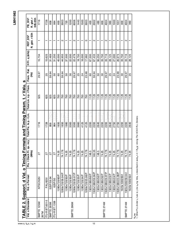
Table 2 shows the recognized input formats with the corre-
sponding reference and feedback divider values, which are
based on the ratio reduced to its lowest factors. Some refer-
ence formats can have up to three sets of compatible divider
values with the same reduced ratio. For example, a 1080p60
input reference has three sets of compatible divider values of
400/1 (reduced), 800/2 and 2000/5. Because the divider val-
ues can directly influence the loop response of the VCXO
PLL, the programmability of these registers can be used ad-
vantageously by the designer. Refer to section
7.0 VCXO PLL
LOOP RESPONSE
for more information.
The HD clock frequency can be selected from
Table 6
and
programmed to HD_FREQ (register 08h). PLL 2 and PLL 3
are used to generate the four different HD clock rates but only
one HD clock can be selected at a time. If the HD_CLK output
is not needed, it can be put in Hi-Z mode by setting HD_HIZ
= 1 (register 08h).
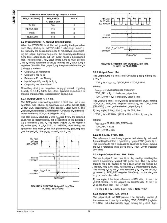
Note:
If 148.35 MHz is selected, it is recommended to follow
the initial programming sequence described in section
2.1
Recommended Start-Up Programming Sequence.
13
www.national.com


 1
1
 2
2
 3
3
 4
4
 5
5
 6
6
 7
7
 8
8
 9
9
 10
10
 11
11
 12
12
 13
13
 14
14
 15
15
 16
16
 17
17
 18
18
 19
19
 20
20
 21
21
 22
22
 23
23
 24
24
 25
25
 26
26
 27
27
 28
28
