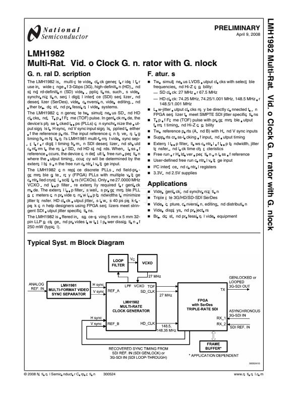
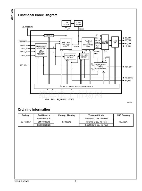
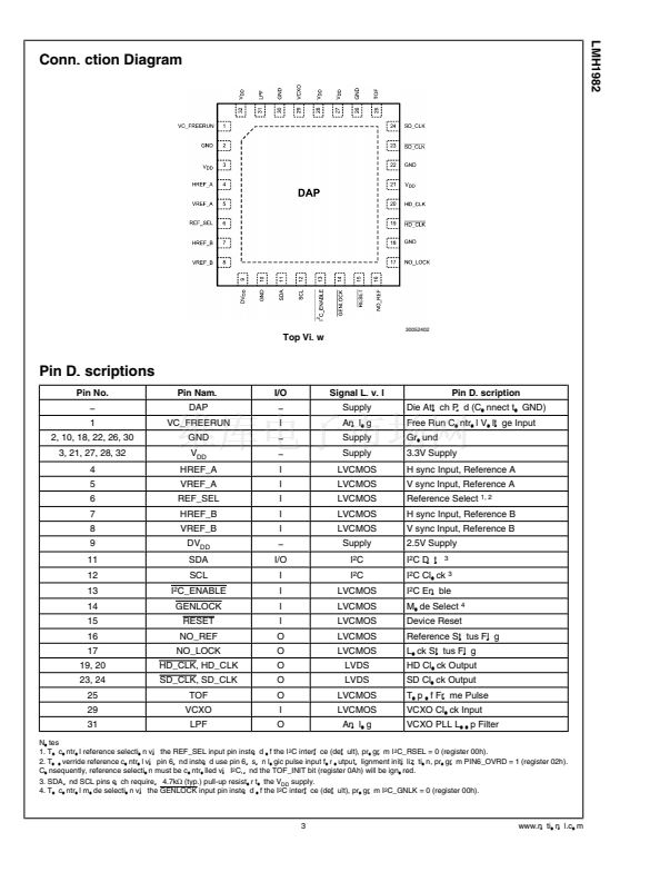
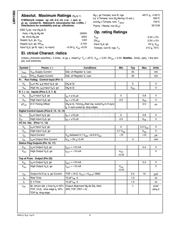
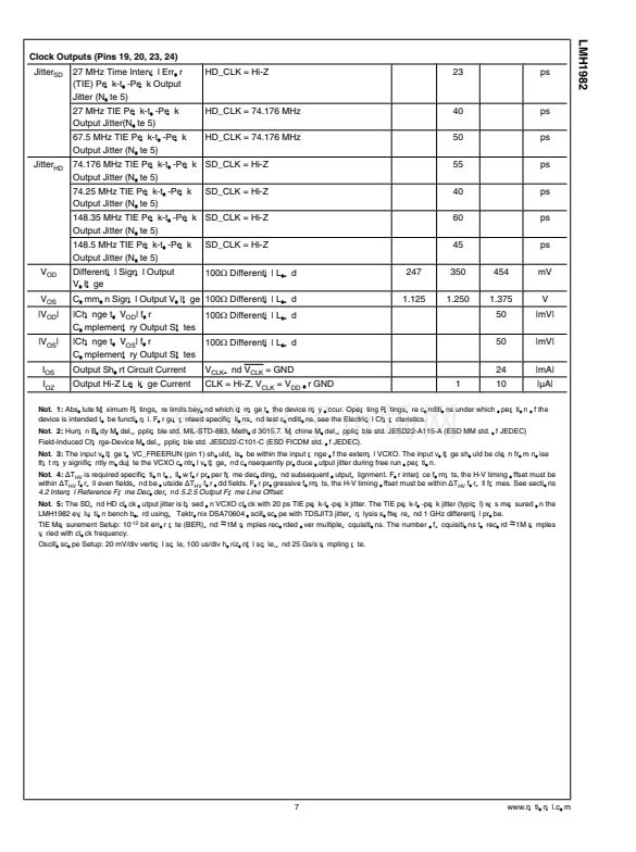
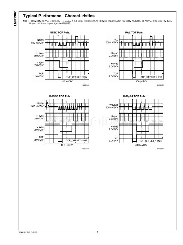
LMH1982
9.1 Genlock And Input Reference Control Registers
REGISTER 00h
Bits 2-0: H Input Error Max Count (H_ERROR)
The H_ERROR bits control the reference detector's error
threshold, which determines the maximum number of missing
H sync pulses before indicating a LOR. See section
6.1.1
Programming the Loss of Reference (LOR) Threshold.
Bit 3: Holdover on Loss of Reference (HOLDOVER)
The HOLDOVER bit controls the operating mode when a loss
of reference occurs. See section
3.2.2 Loss of Reference
(LOR).
Bit 4: Reference Select (RSEL)
The RSEL bit selects either REF_A or REF_B inputs as the
reference to genlock the outputs when I
2
C_RSEL = 1.
RSEL = 0: Select REF_A inputs.
RSEL = 1: Select REF_B inputs.
If PIN6_OVRD = 1 (register 02h), then reference selection
must be controlled by programming RSEL, regardless of
I
2
C_RSEL. When PIN6_OVRD = 0 and I
2
C_RSEL = 0, then
reference selection is controlled using the REF_SEL input pin
and the RSEL bit is ignored.
Bit 5: Reference Select Control via I
2
C (I
2
C_RSEL)
By programming I
2
C_RSEL, reference selection can be con-
trolled either via I
2
C or the REF_SEL input pin.
I
2
C_RSEL = 1: Control reference selection by programming
RSEL.
I
2
C_RSEL = 0: Control reference selection via the
REF_SEL input pin.
Note: If PIN6_OVRD = 1, then reference selection must be
controlled by programming RSEL regardless of I
2
C_RSEL.
Bit 6: Mode Select (GNLK)
The GNLK bit selects the operating mode when I
2
C_GNLK =
1. See section
3.0 MODES OF OPERATION.
GNLK = 0: Selects Free Run mode.
GNLK = 1: Selects Genlock mode.
If I
2
C_GNLK = 0, then the operating mode will be controlled
using the GENLOCK input pin and the GNLK bit will be ig-
nored.
Bit 7: Mode Select via I
2
C (I
2
C_GNLK)
By programming I
2
C_GNLK, mode selection can be con-
trolled either via I
2
C or the GENLOCK input pin.
I
2
C_GNLK = 1: Control mode selection by programming
GNLK.
I
2
C_GNLK = 0: Control mode selection via the GENLOCK
input pin.
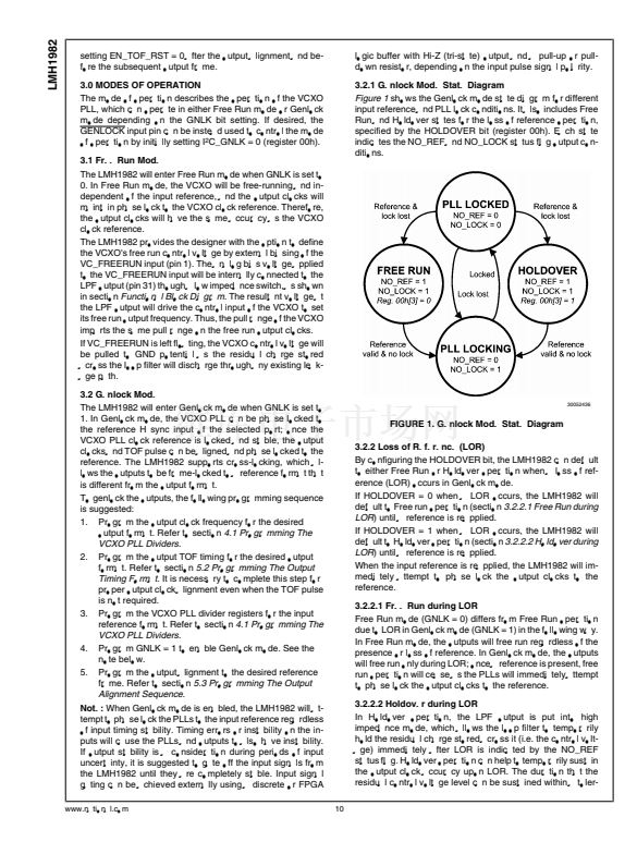
9.2 Genlock Status And Lock Control Register
REGISTER 01h
Bit 0: Reference Status (REF_VALID)
REF_VALID is a read-only bit and indicates the presence or
loss of reference on the selected reference port in Genlock
mode. The NO_REF output flag is an inverted copy of
REF_VALID. See section
6.1 Reference Detection.
REF_VALID = 0: Indicates loss of reference (LOR).
REF_VALID = 1: Indicates valid reference.
In Free Run mode, REF_VALID will be set to 0 to indicate the
absence of any input pulses at the selected HREF port.
www.national.com
20
Bit 1: SD Clock PLL Lock Status (SD_LOCK)
SD_LOCK is a read-only bit and indicates PLL lock status of
the selected SD clock. See section
6.2 PLL Lock Detection.
SD_LOCK = 0: Indicates loss of lock.
SD_LOCK = 1: Indicates valid lock.
Bit 2: HD Clock PLL Lock Status (HD_LOCK)
HD_LOCK is a read-only bit and indicates PLL lock status of
the selected HD clock. See section
6.2 PLL Lock Detection.
HD_LOCK = 0: Indicates loss of lock.
HD_LOCK = 1: Indicates valid lock.
Bits 7-3: Lock Control (LOCK_CTRL)
LOCK_CTRL controls the phase error threshold of the VCXO
PLL lock detector. A larger value for LOCK_CTRL will yield
shorter lock indication time (although not actual lock time) at
the expense of higher output phase error when lock is initially
indicated, whereas a smaller value will yield the opposite ef-
fect. See section
6.2.1 Programming the PLL Lock Thresh-
old.
9.3 Input Control Register
REGISTER 02h
Bit 0: VREF_B Input Signal Polarity (POL_VB)
This bit should be programmed to match the input signal po-
larity at the VREF_B input pin.
POL_VB = 0: Negative polarity or active low signal.
POL_VB = 1: Positive polarity or active high signal.
Bit 1: HREF_B Input Signal Polarity (POL_HB)
This bit should be programmed to match the input signal po-
larity at the HREF_B input pin. The rising edge of the output
clock will be phase locked to the active edge of the H sync
input signal.
POL_HB = 0: Negative polarity or active low signal.
POL_HB = 1: Positive polarity or active high signal.
Bit 2: VREF_A Input Signal Polarity (POL_VA)
This bit should be programmed to match the input signal po-
larity at the VREF_A input pin.
POL_VA = 0: Negative polarity or active low signal.
POL_VA = 1: Positive polarity or active high signal.
Bit 3: HREF_A Input Signal Polarity (POL_HA)
This bit should be programmed to match with the input signal
polarity at HREF_A input pin. The rising edge of the output
clock will be phase locked to the active edge of the H sync
input signal.
POL_HA = 0: Negative polarity or active low signal.
POL_HA = 1: Positive polarity or active high signal.
Bit 4: 27 MHz Reference Control (27M_REF)
Instead of an H sync signal, a 27 MHz clock signal can be
applied to the selected HREF input to phase lock the output
clocks. If a 27 MHz clock is used as a reference, then a value
of 1 should be programmed to 27M_REF, REF_DIV, and
FB_DIV.
27M_REF = 0: H sync input signal.
27M_REF = 1: 27 MHz clock input signal.
Note: The VCXO PLL loop parameters are different between
an H sync signal and a 27 MHz clock signal; therefore, they


 1
1
 2
2
 3
3
 4
4
 5
5
 6
6
 7
7
 8
8
 9
9
 10
10
 11
11
 12
12
 13
13
 14
14
 15
15
 16
16
 17
17
 18
18
 19
19
 20
20
 21
21
 22
22
 23
23
 24
24
 25
25
 26
26
 27
27
 28
28
