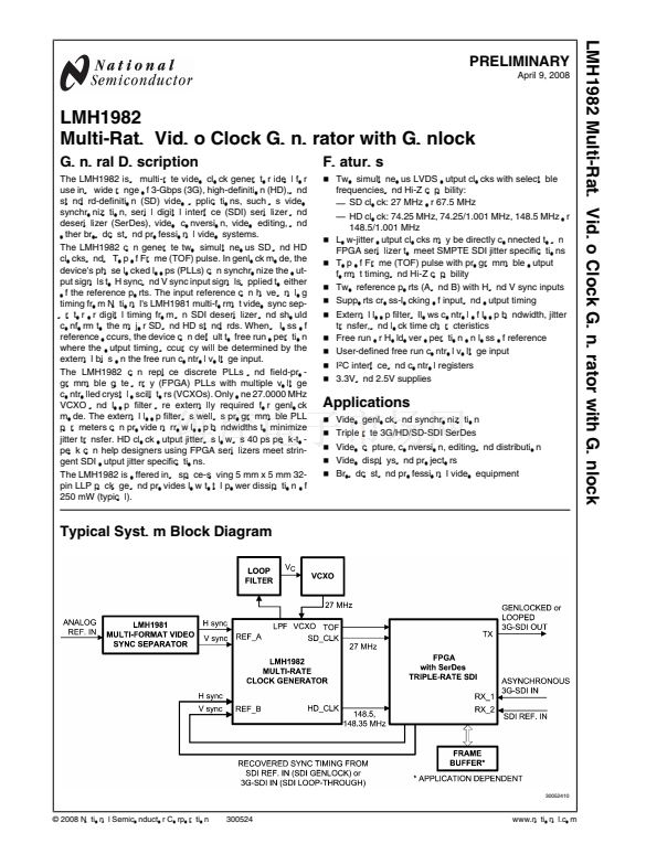
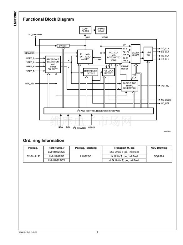
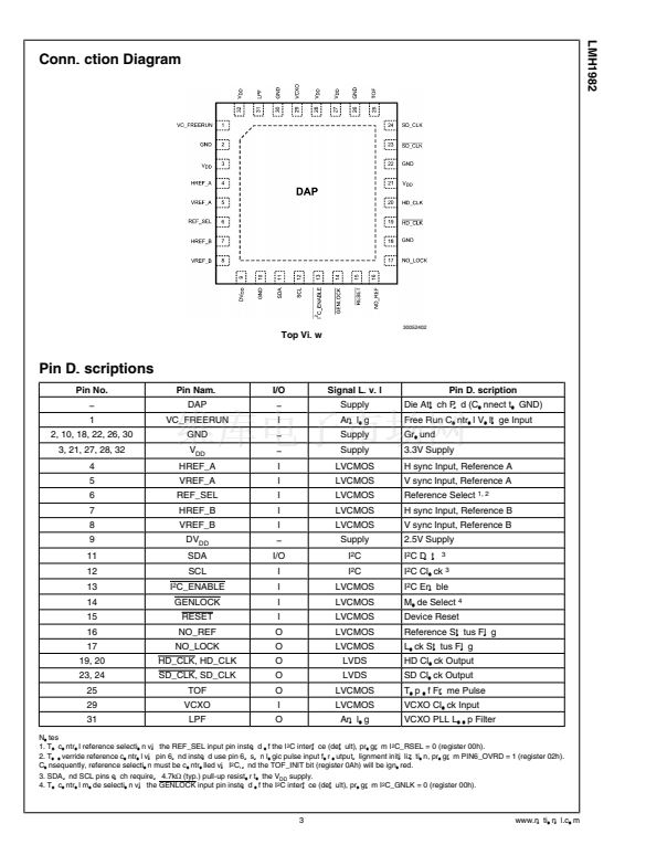
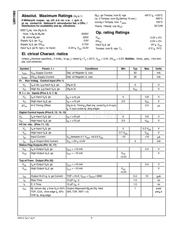
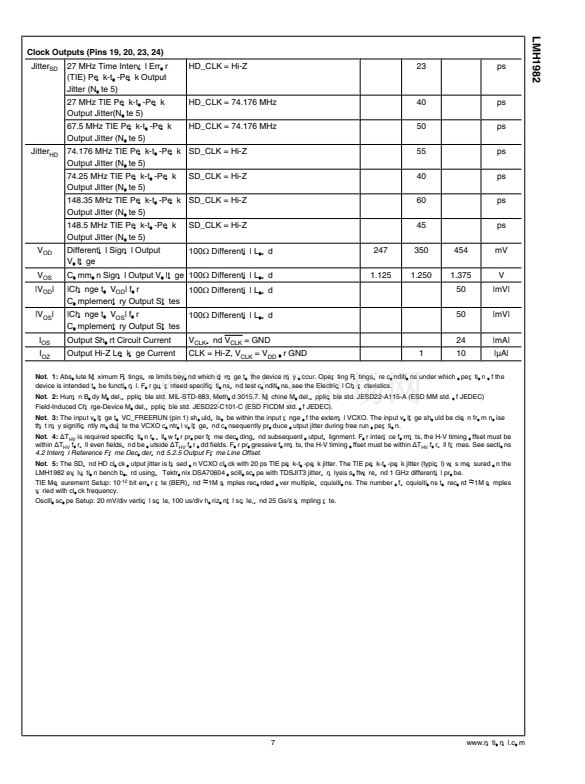
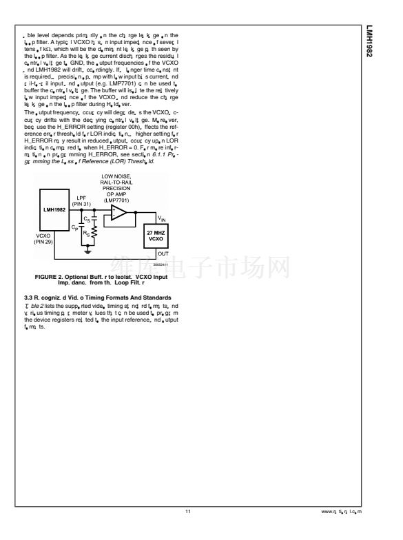
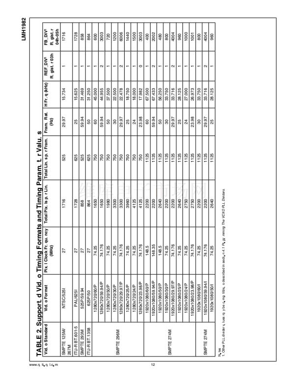
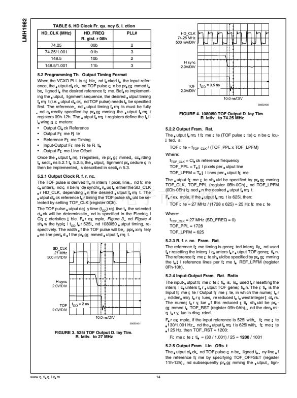
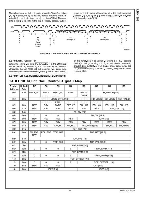
LMH1982
will require different external loop filter components for opti-
mal PLL response.
Bit 5: Pin 6 Override (PIN6_OVRD)
The PIN6_OVRD bit can be programmed to override the de-
fault reference selection capability on pin 6 and instead use
pin 6 as an logic pulse input for output alignment initialization,
which initializes or resets the frame counter programmed to
TOF_RST.
PIN6_OVRD = 0: Allows a logic level input to be applied to
pin 6 for reference selection if RSEL_I
2
C = 0 (register 00h). If
RSEL_I
2
C = 1, then pin 6 is ignored and reference selection
is controlled via I
2
C; additionally, output alignment must be
initialized via I
2
C by programming TOF_INIT and
EN_TOF_RST (register 0Ah).
PIN6_OVRD = 1: Allows an TOF Init pulse to be applied to
pin 6 for output alignment initialization if EN_TOF_RST = 1.
If EN_TOF_RST = 0, then any TOF Init pulse received at pin
6 will be ignored. Additionally, reference selection must be
controlled via I
2
C, regardless of I
2
C_RSEL.
Bits 7-6: Reserved (RSV)
9.4 PLL 1 Divider Register
REGISTER 03h
Bits 1-0: Reference Divider Value (REF_DIV)
REF_DIV selects the reference divider value according to
Table 3.
See section
4.1 Programming The VCXO PLL Di-
viders.
The reference divide value is the denominator of the VCXO
PLL divider ratio:
Feedback divider value / Reference divider value = 27 MHz /
Hsync input frequency
The numerator and denominator values of the divider ratio
must be reduced to their lowest factors before programming
REF_DIV and FB_DIV. These registers must be programmed
correctly for the input timing format in order to phase lock the
27 MHz VCXO PLL and output clocks to the HREF input.
Bits 7-3: Reserved (RSV)
REGISTER 04h
Bits 7-0: Feedback Divide Value (FB_DIV)
This register contains the 8 LSBs of FB_DIV. The feedback
divider value is the numerator of the VCXO PLL divider ratio.
FB_DIV should be programmed using the exact feedback di-
vider value after the divide ratio has been reduced to its lowest
factors. See the description for REF_DIV.
REGISTER 05h
Bits 4-0: Feedback Divide Value (FB_DIV)
This register contains the 5 MSBs of FB_DIV. See the de-
scription for register 04h.
Bits 7-5: These non-programmable bits contain zeros.
9.5 PLL 4 Charge Pump Current Control Registers
REGISTER 06h
Bits 3-0: Charge Pump Current Control for PLL 4 (ICP4)
ICP4 can be programmed to specify the charge pump current
for PLL 4, which generates the 67.5 MHz SD clock.
Note:
Bit 3 is inverted internally, so the default value of 0000b
(0h) actually yields an effective value of 1000b (8h).
Reducing the effective value of the charge pump current will
lower its loop bandwidth at the expense of reduced PLL sta-
bility. An effective value of 0 should not be programmed since
this corresponds to 0 碌A nominal current and will cause PLL
4 to lose phase lock.
Bits 7-4: Reserved (RSV)
REGISTER 07h
Bits 7-0: Reserved (RSV)
9.6 Output Clock And TOF Control Register
REGISTER 08h
Bit 0: SD Clock Output Frequency Select (SD_FREQ)
This bit sets the clock frequency of the SD_CLK output pair.
See section
5.1 Programming The Output Clock Frequen-
cies.
SD_FREQ = 0: Selects 27 MHz from PLL 1.
SD_FREQ = 1: Selects 67.5 MHz from PLL 4.
Bit 1: SD Clock Output Mode (SD_HIZ)
Set the SD_HIZ bit to 1 to put the SD_CLK output pair in high-
impedance (Hi-Z) mode; otherwise, the SD_CLK output will
be enabled.
Bit 3-2: HD Clock Output Frequency Select (HD_FREQ)
These bits set the clock frequency of the HD_CLK output pair.
HD_FREQ = 00b: Selects 74.25 MHz from PLL 2.
HD_FREQ = 01b: Selects 74.176 MHz from PLL 3.
HD_FREQ = 10b: Selects 148.5 MHz from PLL 2.
HD_FREQ = 11b: Selects 148.35 MHz from PLL 3.
Bit 4: HD Clock Output Mode (HD_HIZ)
Set the HD_HIZ bit to 1 to put the HD_CLK output pair in high-
impedance (Hi-Z) mode; otherwise, the HD_CLK output will
be enabled.
Bit 5: Top of Frame Output Mode (TOF_HIZ)
Set the TOF_HIZ bit to 1 to put the TOF output pin in high-
impedance (Hi-Z) mode; otherwise, the output will be en-
abled.
Bits 7-6: Reserved (RSV)
9.7 TOF Configuration Registers
REGISTER 09h
Bits 7-0: TOF Reset (TOF_RST)
This register contains the 8 LSBs of TOF_RST. When the
VCXO PLL is phase locked to the reference, both H sync and
V sync inputs are used to reset the frame-based counters
used for output TOF generation. The numerator value of the
reduced frame rate ratio should be programmed to
TOF_RST. See section
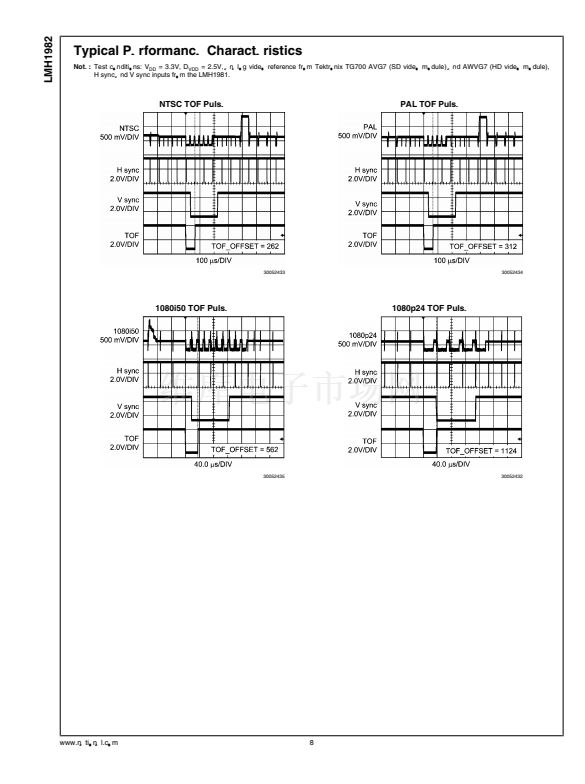
5.2.4 Input-Output Frame Rate Ra-
tio.
For example, if the input timing is NTSC and the desired out-
put timing is PAL, then a value of 1200 (decimal) should be
programmed to TOF_RST (30/1.001 Hz / 25 Hz =
1200
/
1001).
Once TOF_RST is programmed, it must be properly initialized
by either programming TOF_INIT or otherwise using an ex-
ternal TOF Init pulse (when PIN6_OVRD = 1).
21
www.national.com


 1
1
 2
2
 3
3
 4
4
 5
5
 6
6
 7
7
 8
8
 9
9
 10
10
 11
11
 12
12
 13
13
 14
14
 15
15
 16
16
 17
17
 18
18
 19
19
 20
20
 21
21
 22
22
 23
23
 24
24
 25
25
 26
26
 27
27
 28
28
