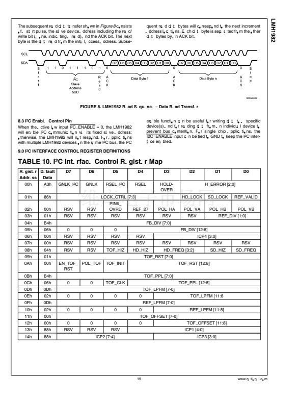
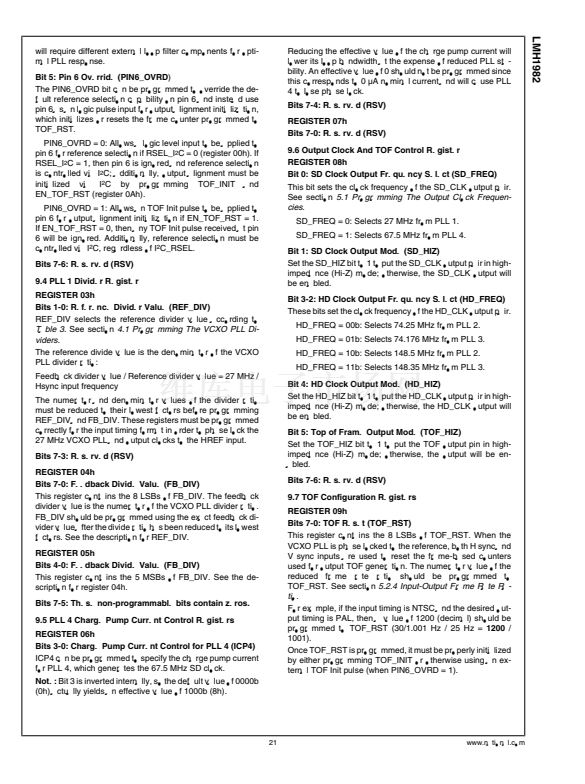
鈥?/div>
I/O
I
I
I
I
O
O
O
O
O
I
O
Signal Level
Supply
Analog
Supply
Supply
LVCMOS
LVCMOS
LVCMOS
LVCMOS
LVCMOS
Supply
I
2
C
I
2
C
LVCMOS
LVCMOS
LVCMOS
LVCMOS
LVCMOS
LVDS
LVDS
LVCMOS
LVCMOS
Analog
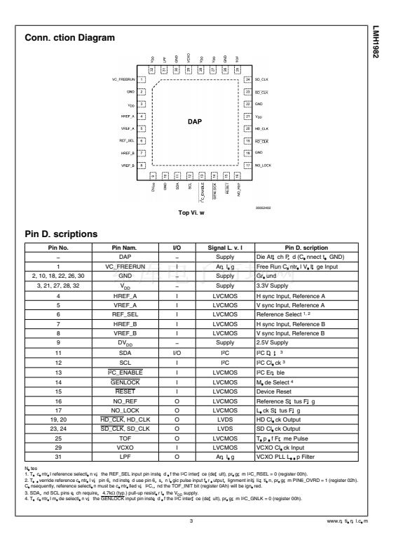
Pin Description
Die Attach Pad (Connect to GND)
Free Run Control Voltage Input
Ground
3.3V Supply
H sync Input, Reference A
V sync Input, Reference A
Reference Select
1, 2
H sync Input, Reference B
V sync Input, Reference B
2.5V Supply
I
2
C Data
3
I
2
C Clock
3
I
2
C Enable
Mode Select
4
Device Reset
Reference Status Flag
Lock Status Flag
HD Clock Output
SD Clock Output
Top of Frame Pulse
VCXO Clock Input
VCXO PLL Loop Filter
Notes
1. To control reference selection via the REF_SEL input pin instead of the I
2
C interface (default), program I
2
C_RSEL = 0 (register 00h).
2. To override reference control via pin 6 and instead use pin 6 as an logic pulse input for output alignment initialization, program PIN6_OVRD = 1 (register 02h).
Consequently, reference selection must be controlled via I
2
C, and the TOF_INIT bit (register 0Ah) will be ignored.
3. SDA and SCL pins each require a 4.7k鈩?/div>
(typ.)
pull-up resistor to the V
DD
supply.
4. To control mode selection via the GENLOCK input pin instead of the I
2
C interface (default), program I
2
C_GNLK = 0 (register 00h).
3
www.national.com


 1
1
 2
2
 3
3
 4
4
 5
5
 6
6
 7
7
 8
8
 9
9
 10
10
 11
11
 12
12
 13
13
 14
14
 15
15
 16
16
 17
17
 18
18
 19
19
 20
20
 21
21
 22
22
 23
23
 24
24
 25
25
 26
26
 27
27
 28
28
