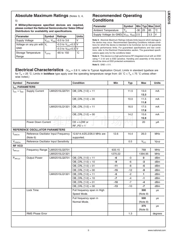
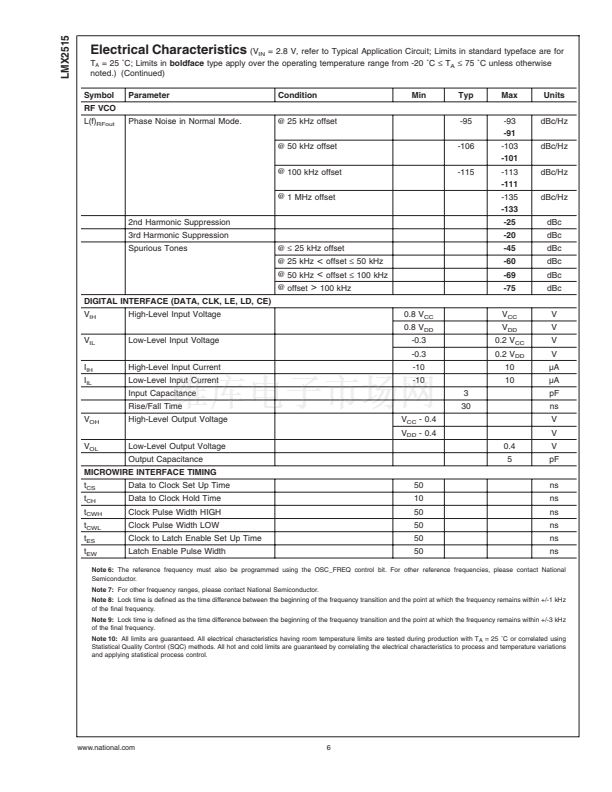
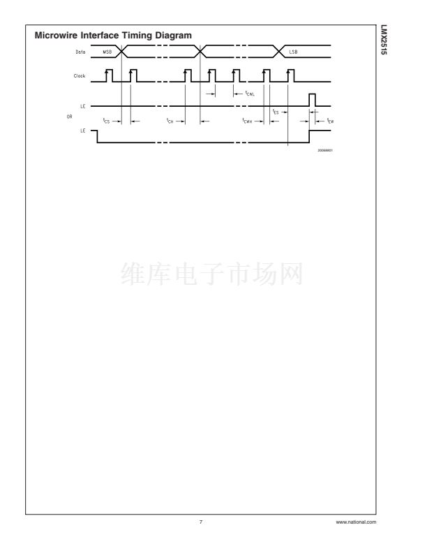
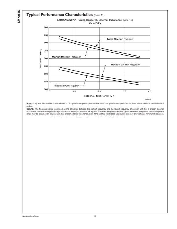
LMX2515
Functional Description
CE pin
HIGH
HIGH
LOW
LOW
VCO SELECTION
RF_PD Bit
0
1
0
1
(Continued)
TABLE 1. Power Down Modes
Mode
Active
Not Active
Not Active
Not Active
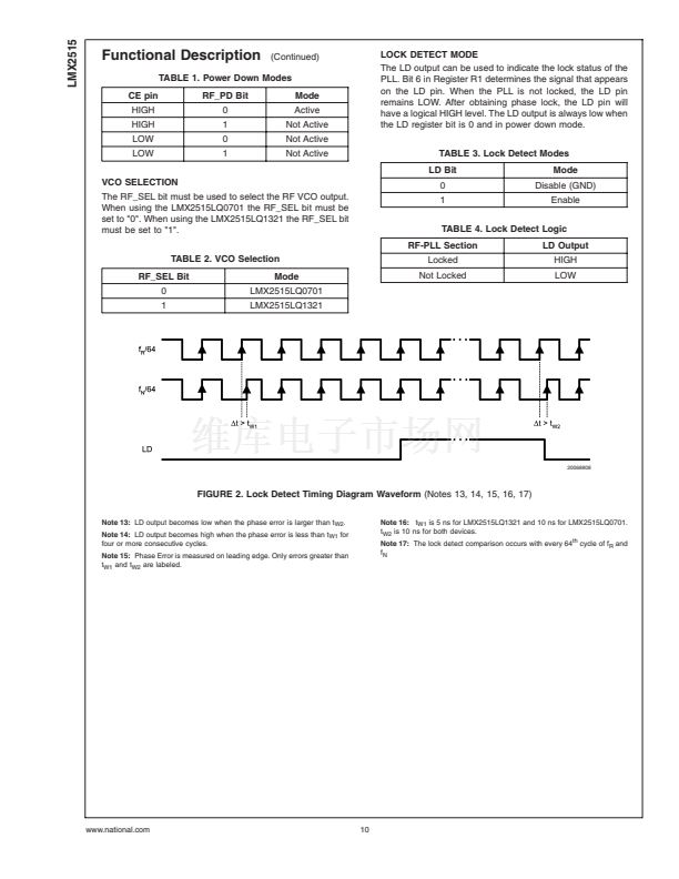
LOCK DETECT MODE
The LD output can be used to indicate the lock status of the
PLL. Bit 6 in Register R1 determines the signal that appears
on the LD pin. When the PLL is not locked, the LD pin
remains LOW. After obtaining phase lock, the LD pin will
have a logical HIGH level. The LD output is always low when
the LD register bit is 0 and in power down mode.
TABLE 3. Lock Detect Modes
LD Bit
0
1
Mode
Disable (GND)
Enable
The RF_SEL bit must be used to select the RF VCO output.
When using the LMX2515LQ0701 the RF_SEL bit must be
set to "0". When using the LMX2515LQ1321 the RF_SEL bit
must be set to "1".
TABLE 2. VCO Selection
RF_SEL Bit
0
1
Mode
LMX2515LQ0701
LMX2515LQ1321
TABLE 4. Lock Detect Logic
RF-PLL Section
Locked
Not Locked
LD Output
HIGH
LOW
20068808
FIGURE 2. Lock Detect Timing Diagram Waveform
(Notes 13, 14, 15, 16, 17)
Note 13:
LD output becomes low when the phase error is larger than t
W2
.
Note 14:
LD output becomes high when the phase error is less than t
W1
for
four or more consecutive cycles.
Note 15:
Phase Error is measured on leading edge. Only errors greater than
t
W1
and t
W2
are labeled.
Note 16:
t
W1
is 5 ns for LMX2515LQ1321 and 10 ns for LMX2515LQ0701.
t
W2
is 10 ns for both devices.
Note 17:
The lock detect comparison occurs with every 64
th
cycle of f
R
and
f
N
www.national.com
10


 1
1
 2
2
 3
3
 4
4
 5
5
 6
6
 7
7
 8
8
 9
9
 10
10
 11
11
 12
12
 13
13
 14
14
 15
15
 16
16
 17
17
