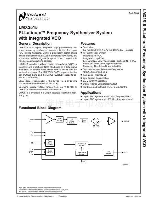
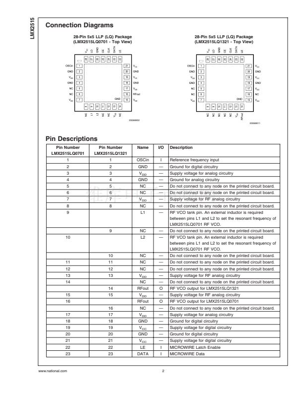
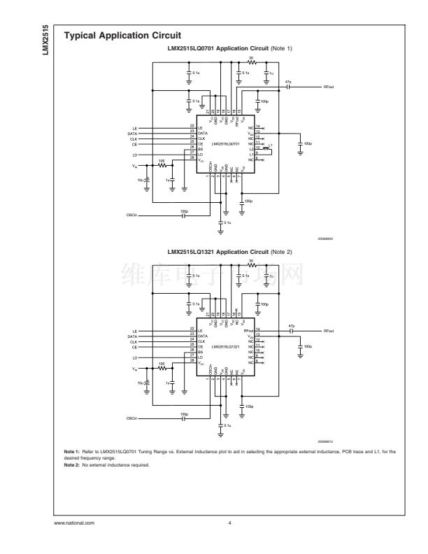
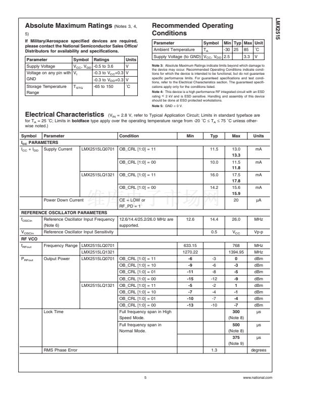
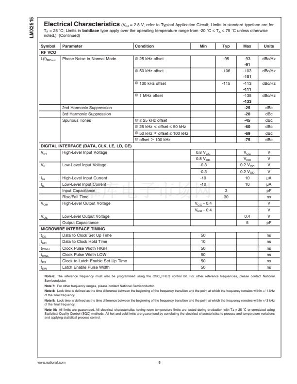
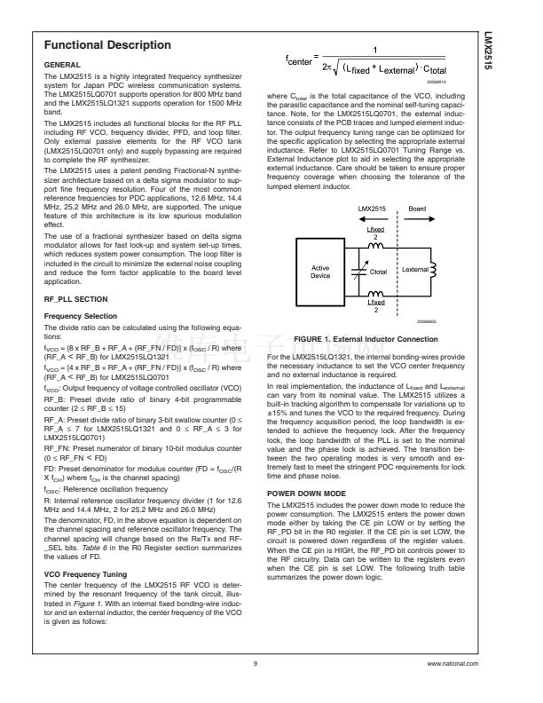
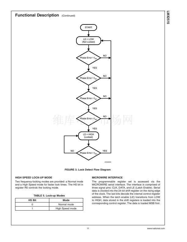
LMX2515
Programming Description
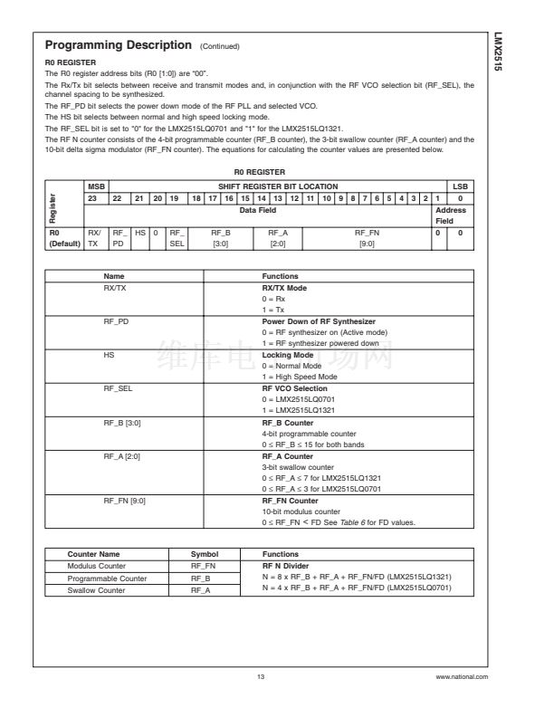
GENERAL PROGRAMMING INFORMATION
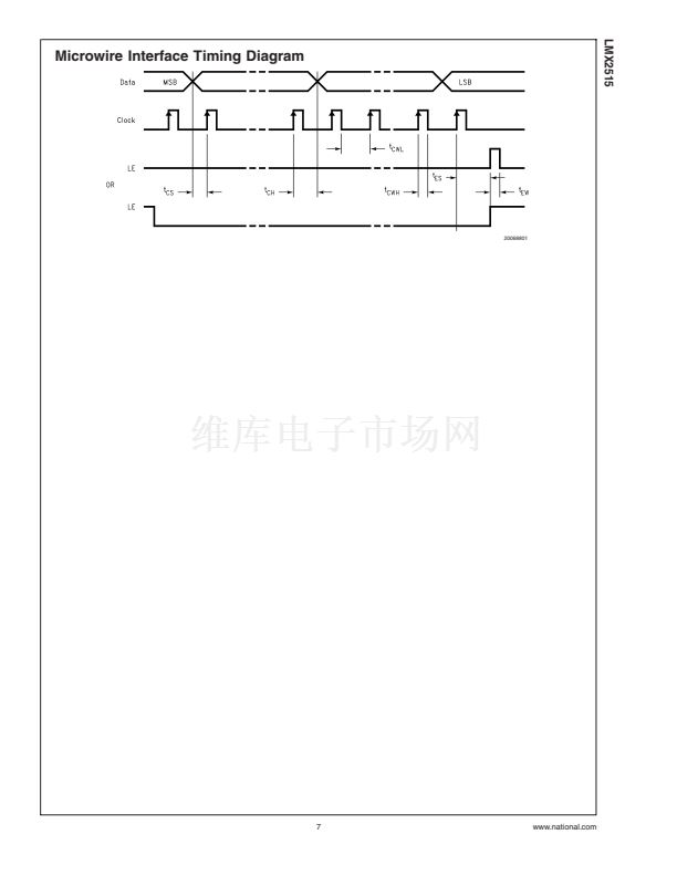
The serial interface has a 24-bit shift register to store the incoming data bits temporarily. The incoming data is first loaded into the
shift register from MSB to LSB. The data is shifted at the rising edge of the clock signal. When the latch enable signal transitions
from LOW to HIGH, the data stored in shift register is transferred to the proper register depending on the address bit setting. The
selection of the particular register is determined by the control bits indicated in boldface text.
At initial start-up, the MICROWIRE loading requires three default words (registers R2, loaded first, to R0, loaded last). After the
device has been initially programmed, the RF VCO frequency can be changed using a single register (R0).
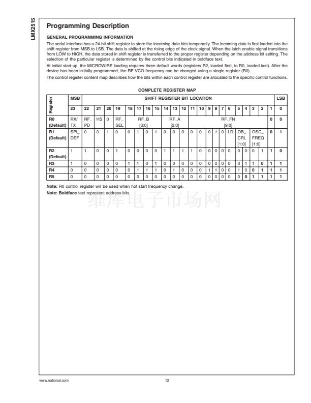
The control register content map describes how the bits within each control register are allocated to the specific control functions.
COMPLETE REGISTER MAP
Register
MSB
23
22
21
20 19
RF_
SEL
0
0
SHIFT REGISTER BIT LOCATION
18 17 16 15 14 13 12 11 10 9 8 7 6
RF_B
[3:0]
1
0
1
0
RF_A
[2:0]
0
0
0
0
RF_FN
[9:0]
0 1 0 LD OB_
CRL
[1:0]
0 0 0 0
0 0 0 0
1 1 0 0
0 0 0 0
0
0
1
0
0
1
0
0
OSC_
FREQ
[1:0]
0
1
0
1
1
0
1
1
5
4
3
2
1
0
0
LSB
0
0
1
R0
RX/
(Default)
TX
R1
SPI_
(Default)
DEF
R2
1
(Default)
R3
R4
R5
1
0
0
RF_ HS 0
PD
0
0
1
1
0
0
0
0
0
0
0
0
0
0
0
1
0
0
0
0
1
0
0
0
1
1
0
0
0
1
0
0
1
1
0
1
0
0
0
1
0
1
0
1
0
0
0
1
0
0
0
0
0
0
0
1
1
1
1
0
1
1
1
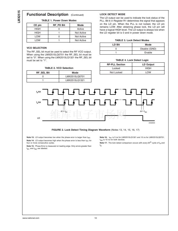
Note:
R0 control register will be used when hot start frequency change.
Note: Boldface
text represent address bits.
www.national.com
12


 1
1
 2
2
 3
3
 4
4
 5
5
 6
6
 7
7
 8
8
 9
9
 10
10
 11
11
 12
12
 13
13
 14
14
 15
15
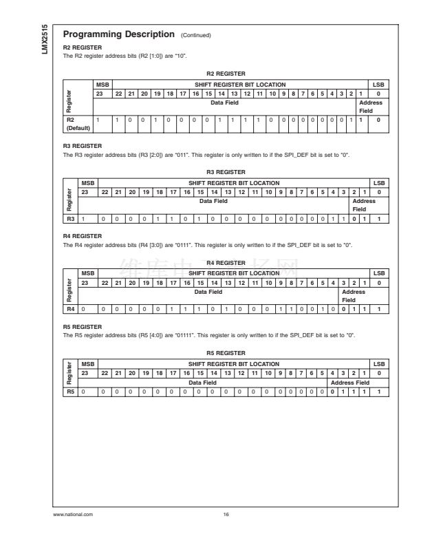 16
16
 17
17
