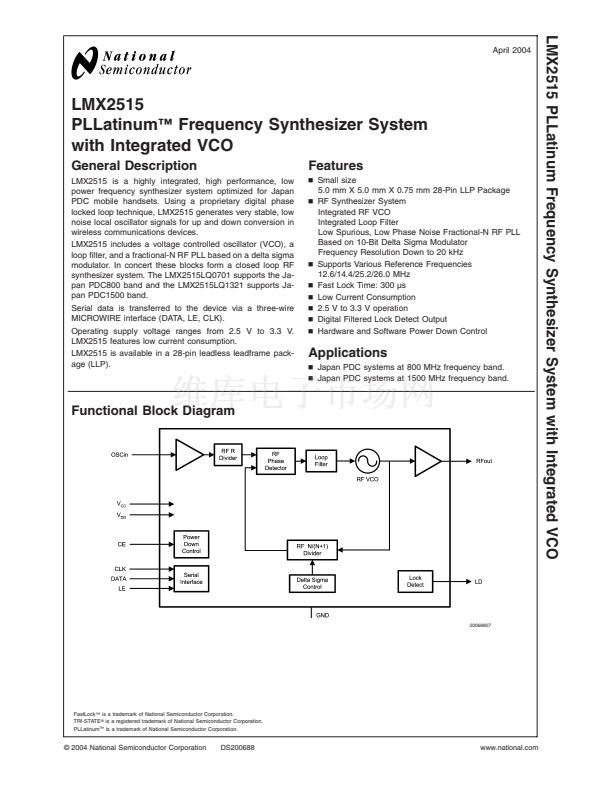
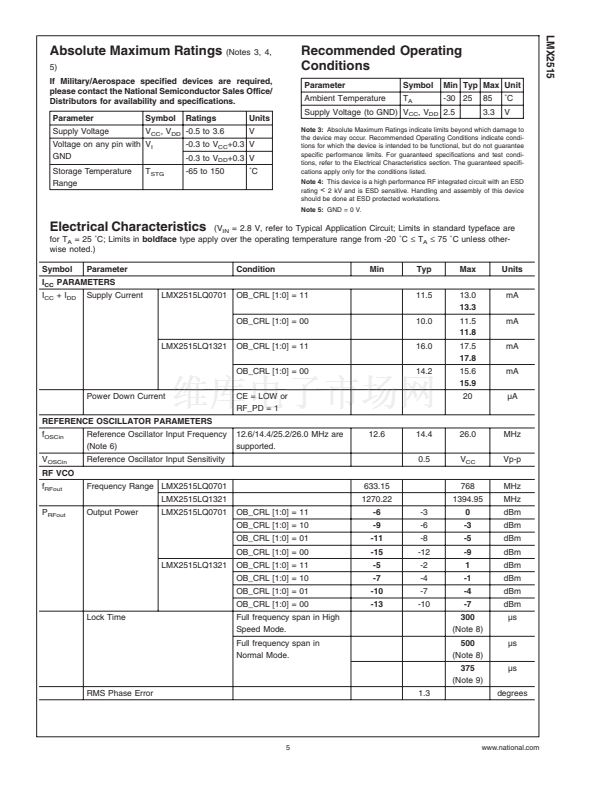
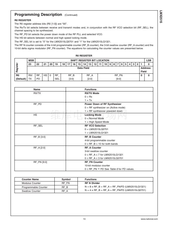
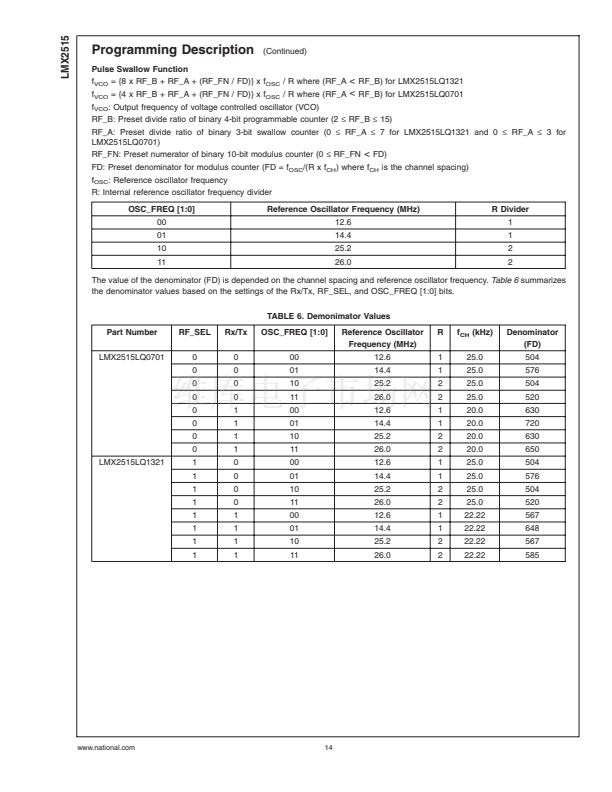
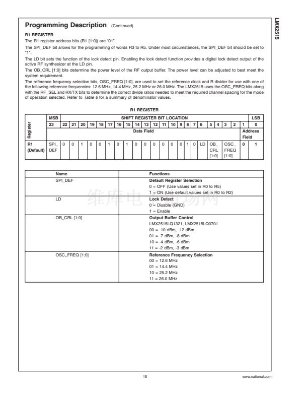
LMX2515
Functional Description
(Continued)
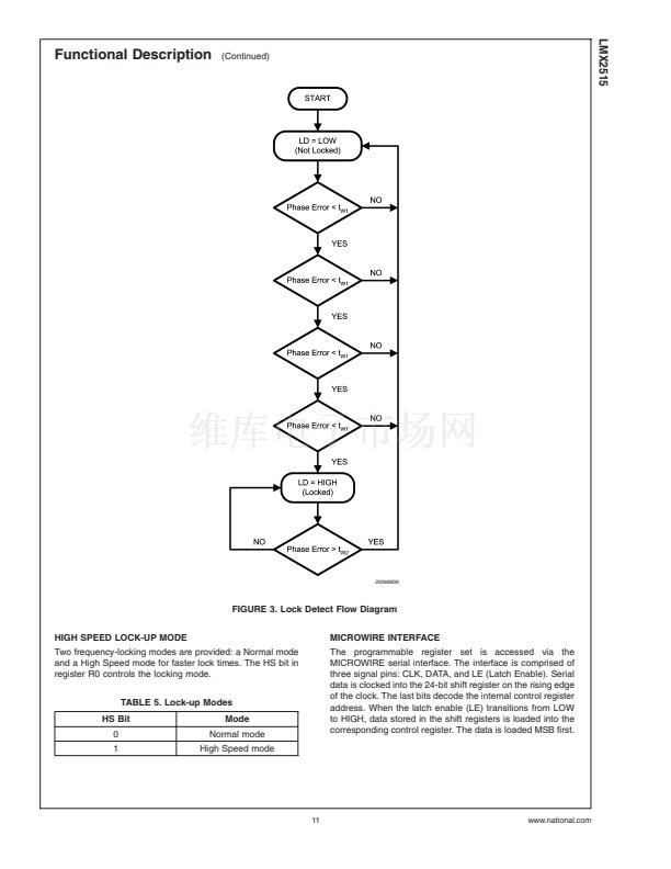
20068809
FIGURE 3. Lock Detect Flow Diagram
HIGH SPEED LOCK-UP MODE
Two frequency-locking modes are provided: a Normal mode
and a High Speed mode for faster lock times. The HS bit in
register R0 controls the locking mode.
TABLE 5. Lock-up Modes
HS Bit
0
1
Mode
Normal mode
High Speed mode
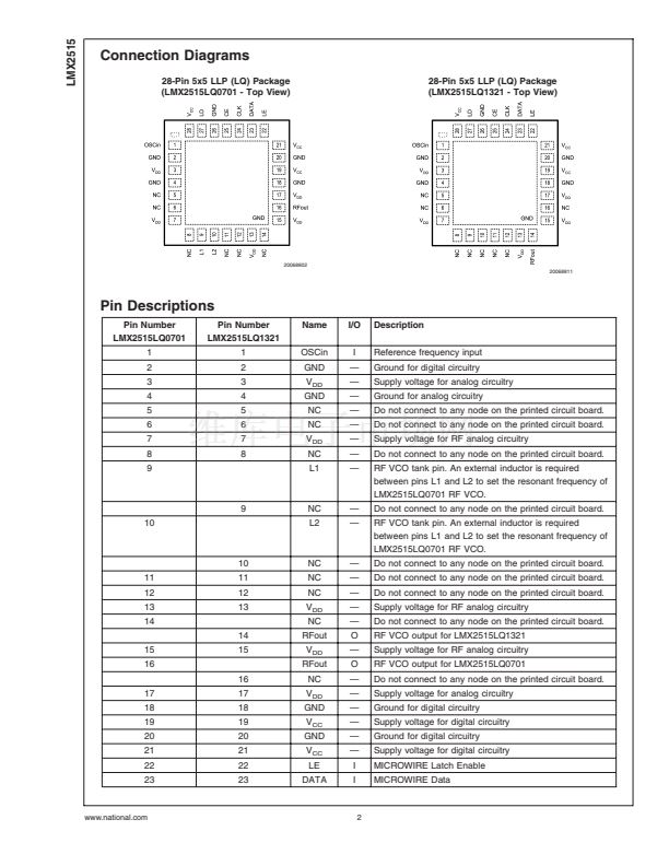
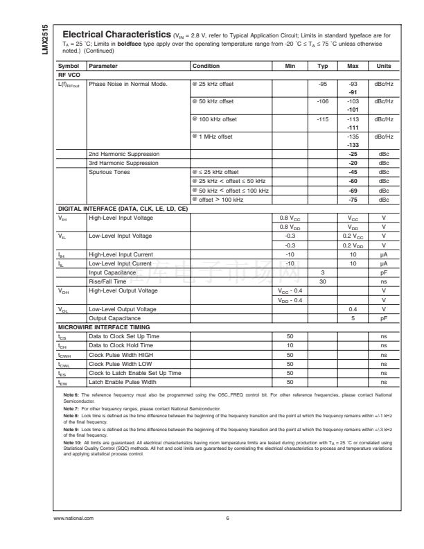
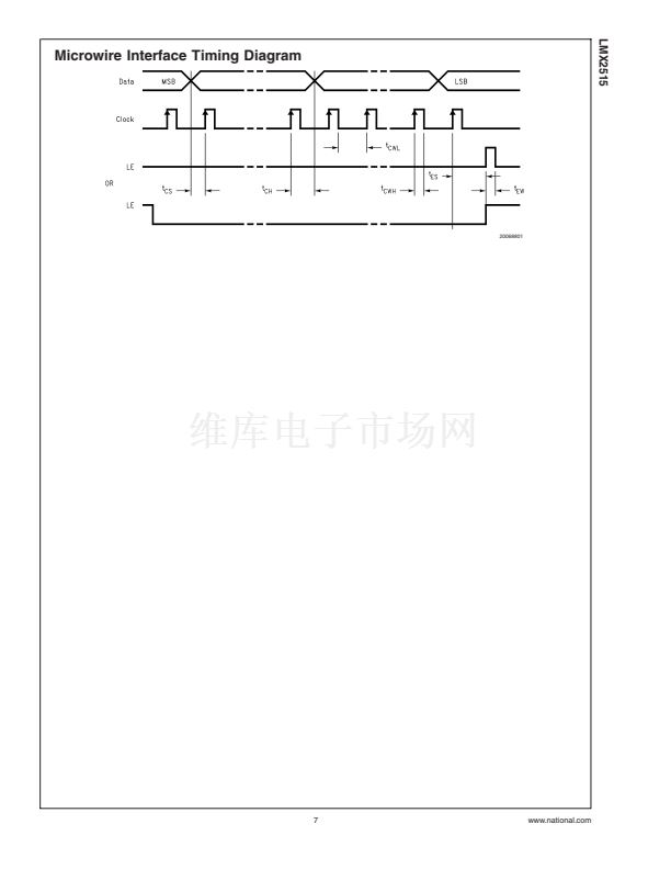
MICROWIRE INTERFACE
The programmable register set is accessed via the
MICROWIRE serial interface. The interface is comprised of
three signal pins: CLK, DATA, and LE (Latch Enable). Serial
data is clocked into the 24-bit shift register on the rising edge
of the clock. The last bits decode the internal control register
address. When the latch enable (LE) transitions from LOW
to HIGH, data stored in the shift registers is loaded into the
corresponding control register. The data is loaded MSB first.
11
www.national.com


 1
1
 2
2
 3
3
 4
4
 5
5
 6
6
 7
7
 8
8
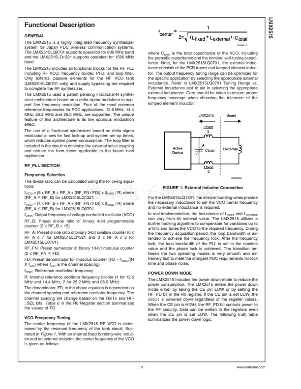 9
9
 10
10
 11
11
 12
12
 13
13
 14
14
 15
15
 16
16
 17
17
