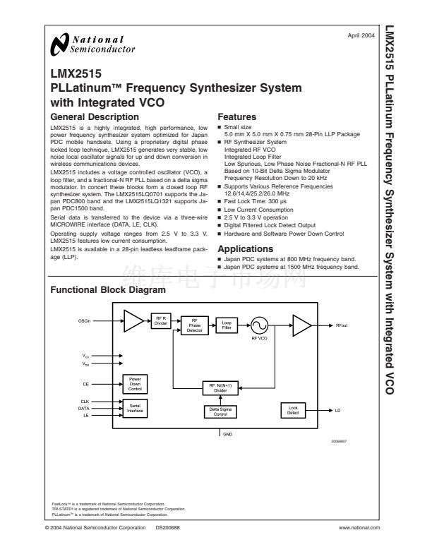
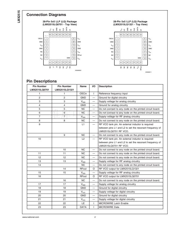
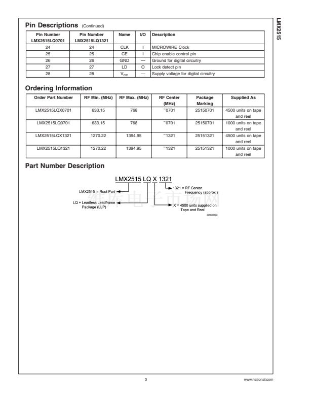
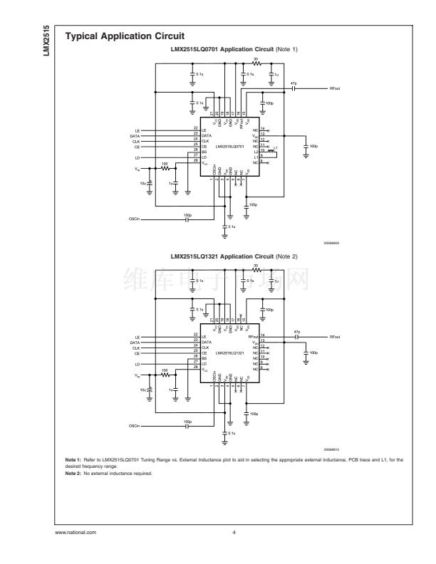
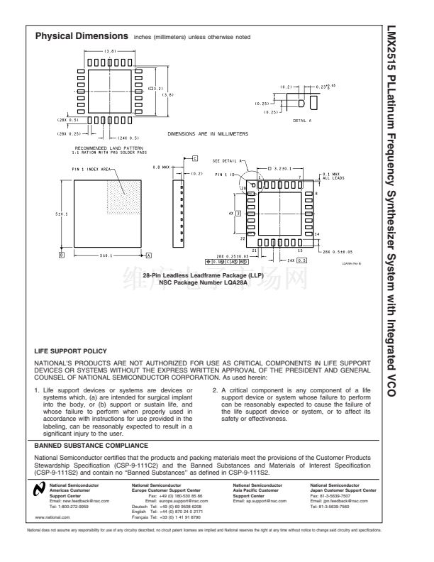
LMX2515
Absolute Maximum Ratings
(Notes 3, 4,
5)
If Military/Aerospace specified devices are required,
please contact the National Semiconductor Sales Office/
Distributors for availability and specifications.
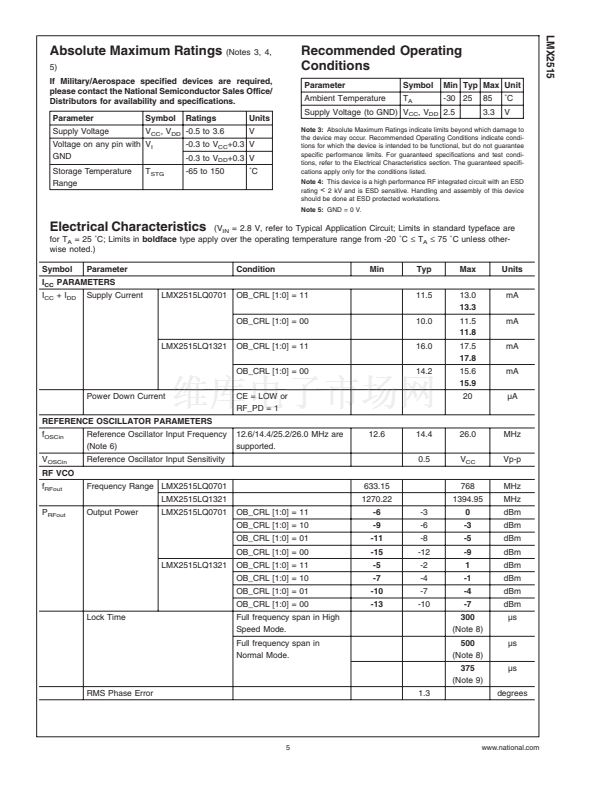
Parameter
Supply Voltage
Symbol
Ratings
Units
V
Recommended Operating
Conditions
Parameter
Ambient Temperature
Symbol
T
A
Min Typ Max Unit
-30 25
85
3.3
藲C
V
Supply Voltage (to GND) V
CC
, V
DD
2.5
V
CC
, V
DD
-0.5 to 3.6
Voltage on any pin with V
I
GND
Storage Temperature
Range
T
STG
-0.3 to V
CC
+0.3 V
-0.3 to V
DD
+0.3 V
-65 to 150
藲C
Note 3:
Absolute Maximum Ratings indicate limits beyond which damage to
the device may occur. Recommended Operating Conditions indicate condi-
tions for which the device is intended to be functional, but do not guarantee
specific performance limits. For guaranteed specifications and test condi-
tions, refer to the Electrical Characteristics section. The guaranteed specifi-
cations apply only for the conditions listed.
Note 4:
This device is a high performance RF integrated circuit with an ESD
rating
<
2 kV and is ESD sensitive. Handling and assembly of this device
should be done at ESD protected workstations.
Note 5:
GND = 0 V.
(V
IN
= 2.8 V, refer to Typical Application Circuit; Limits in standard typeface are
for T
A
= 25 藲C; Limits in
boldface
type apply over the operating temperature range from -20 藲C
鈮?/div>
T
A
鈮?/div>
75 藲C unless other-
wise noted.)
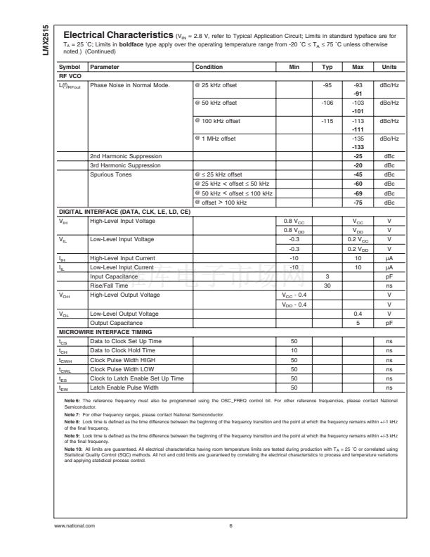
Symbol
I
CC
+ I
DD
Parameter
Supply Current
LMX2515LQ0701
Condition
OB_CRL [1:0] = 11
OB_CRL [1:0] = 00
LMX2515LQ1321
OB_CRL [1:0] = 11
OB_CRL [1:0] = 00
Power Down Current
REFERENCE OSCILLATOR PARAMETERS
f
OSCin
V
OSCin
RF VCO
f
RFout
P
RFout
Frequency Range LMX2515LQ0701
LMX2515LQ1321
Output Power
LMX2515LQ0701
OB_CRL [1:0] = 11
OB_CRL [1:0] = 10
OB_CRL [1:0] = 01
OB_CRL [1:0] = 00
LMX2515LQ1321
OB_CRL [1:0] = 11
OB_CRL [1:0] = 10
OB_CRL [1:0] = 01
OB_CRL [1:0] = 00
Lock Time
Full frequency span in High
Speed Mode.
Full frequency span in
Normal Mode.
633.15
1270.22
-6
-9
-11
-15
-5
-7
-10
-13
-3
-6
-8
-12
-2
-4
-7
-10
768
1394.95
0
-3
-5
-9
1
-1
-4
-7
300
(Note 8)
500
(Note 8)
375
(Note 9)
RMS Phase Error
1.3
MHz
MHz
dBm
dBm
dBm
dBm
dBm
dBm
dBm
dBm
碌s
碌s
碌s
degrees
Reference Oscillator Input Frequency
(Note 6)
Reference Oscillator Input Sensitivity
12.6/14.4/25.2/26.0 MHz are
supported.
12.6
14.4
0.5
26.0
V
CC
MHz
Vp-p
CE = LOW or
RF_PD = 1
Min
Typ
11.5
10.0
16.0
14.2
Max
13.0
13.3
11.5
11.8
17.5
17.8
15.6
15.9
20
Units
mA
mA
mA
mA
碌A
Electrical Characteristics
I
CC
PARAMETERS
5
www.national.com


 1
1
 2
2
 3
3
 4
4
 5
5
 6
6
 7
7
 8
8
 9
9
 10
10
 11
11
 12
12
 13
13
 14
14
 15
15
 16
16
 17
17
