鈮?/div>
13.2V ranges. These
ranges correspond to nominal V
DD
of 5V and 12V, respectively.
Guaranteed by design.
V
OT
is guaranteed by design to always be higher than V
PWM(max)
.
Logic time base and PWM frequency. For other values of C
F
, f(Hz) = 30Hz
0.1
碌
F
, where C is in
碌F.
C
Timing Diagrams
V
OT
0.7V
DD
V
T1
V
T2
V
SLP
0.3V
DD
80%
50%
40%
70%
40%
100%
Input
Signal
Range
30%
0%
V
IH
V
IL
0V
V
OTF
V
OH
V
OL
0V
F
V
OUT
V
OH
V
OL
0V
50%
80%
40%
70%
0%
100%
40%
A
t
PWM
B
C
D
E
t
STARTUP
G
Output
Duty Cycle
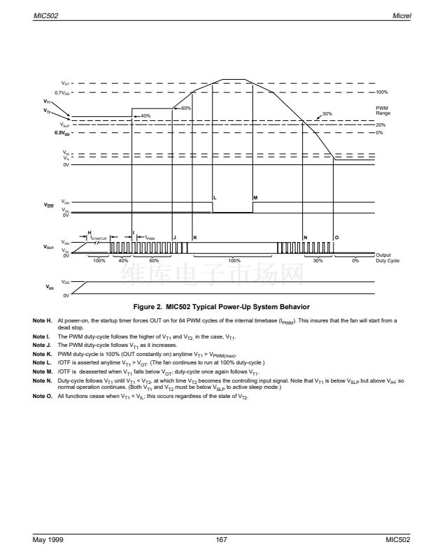
Figure 1. Typical System Behavior
Note A.
Output duty-cycle is initially determined by V
T1
, as it is greater than V
T2
.
Note B.
PWM duty-cycle follows V
T1
as it increases.
Note C.
V
T1
drops below V
T2
. V
T2
now determines the output duty-cycle.
Note D.
The PWM duty-cycle follows V
T2
as it increases.
Note E.
Note F.
Both V
T1
and V
T2
decrease below V
SLP
but above V
IL
. The device enters sleep mode.
The PWM 鈥榳akes up鈥?because one of the control inputs (V
T1
in this case) has risen above V
WAKE
. The startup timer is triggered, forcing OUT
high for 64 clock periods. (V
WAKE
= V
SLP
+ V
HYST
. See 鈥淓lectrical Characteristics.鈥?
Note G.
Following the startup interval, the PWM duty-cycle is the higher of V
T1
and V
T2
.
MIC502
166
May 1999


 1
1
 2
2
 3
3
 4
4
 5
5
 6
6
 7
7
 8
8
 9
9
 10
10
 11
11
