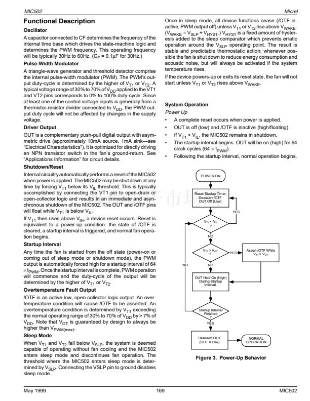
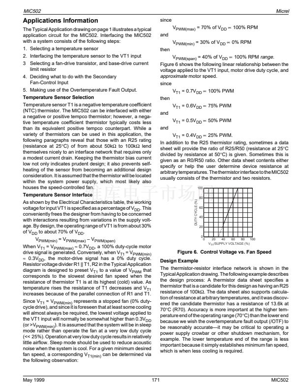
MIC502
The design consists soley of choosing the value R
BASE
in
Figures 7 and 8. To minimize on-chip power dissipation in the
MIC502, the value of R
BASE
should be determined by the
power supply voltage. The Electrical Characteristics table
specifies a minimum output current of 10mA. However,
different output voltage drops (V
DD
鈥?V
OUT
) exist for 5V vs.
12V operation. The value R
BASE
should be as high as
possible for a given required transistor base-drive current in
order to reduce on-chip power dissipation.
Referring to the 鈥淭ypical Application鈥?and to the 鈥淓lectrical
Characteristics鈥?table, the value for R
BASE
is calculated as
follows. For V
DD
= 5V systems, I
OH
of OUT (pin 7) is
guaranteed to be a minimum of 10mA with a V
OH
of 2.4V.
R
BASE
then equals (2.4V 鈥?V
BE
)
梅
10mA = 170鈩?
For V
DD
= 12V systems, R
BASE
= (3.4 鈥?0.7)
梅
0.01 = 250鈩?
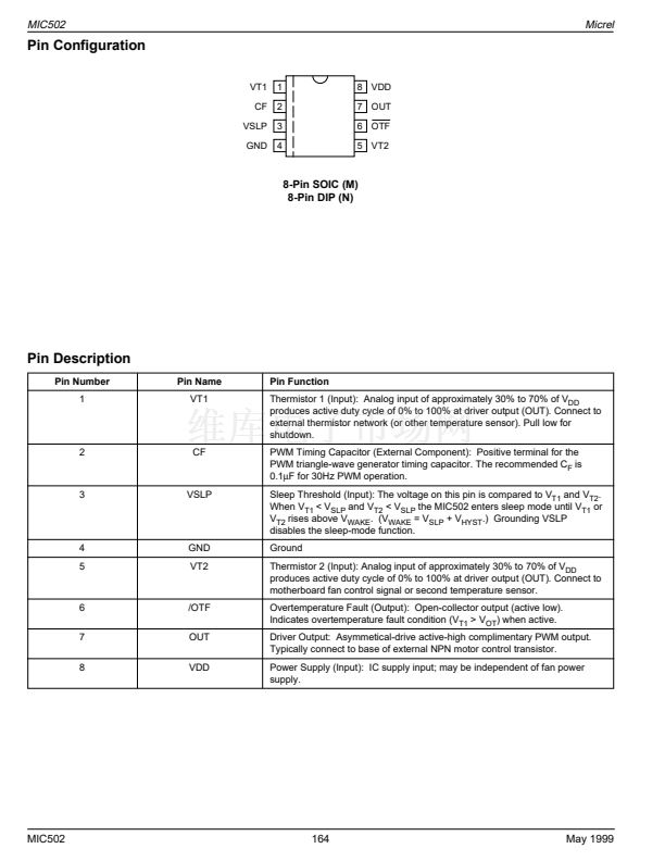
Overtemperature Fault Output
The /OTF output, pin 6, is an open-collector NPN output. It is
compatible with CMOS and TTL logic and is intended for
Micrel
alerting a system about an overtemperature condition or
triggering a power supply crowbar circuit. If V
DD
for the
MIC502 is 5V the output should not be pulled to a higher
voltage. This output can sink up to 2mA and remain compat-
ible with the TTL logic-low level.
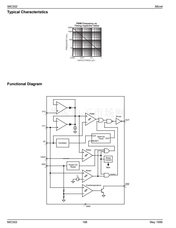
Timing Capacitors vs. PWM Frequency
The recommended C
F
(see first page) is 0.1碌F for opertaion
at a PWM frequency of 30Hz. This frequency is factory
trimmed within
卤3Hz
using a 0.1% accurate capacitor. If it is
desired to operate at a different frequency, the new value for
C
F
is calculated as follows:
3
, where C is in
碌F
and f is in Hz.
f
The composition, voltage rating, ESR, etc., parameters of the
capacitor are not critical. However, if tight control of frequency
vs. temperature is an issue, the temperature coefficient may
become a consideration.
C=
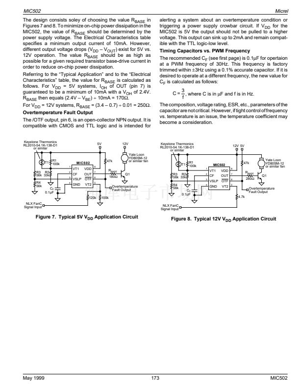
Keystone Thermonics
RL2010-54.1K-138-D1
or similar
5V
12V
Yate Loon
YD80SM-12
or similar fan
Keystone Thermonics
RL2010-54.1K-138-D1
or similar
12V 5V
T1
R3 R2
56k 33k
R4
56k
R1
100k
1
2
3
4
MIC502
VT1
CF
GND
VDD
OUT
VT2
8
7
6
5
47k
R
BASE
180鈩?/div>
T1
Q1
R3 R2
56k 33k
R4
56k
R1
100k
1
2
3
4
MIC502
VT1
CF
GND
VDD
OUT
VT2
8
7
6
5
47k
R
BASE
280鈩?/div>
Yate Loon
YD80SM-12
or similar fan
Q1
VSLP OTF
VSLP OTF
C
F
0.1碌F
120k
100k
Overtemperature
Fault Output
C
F
0.1碌F
Overtemperature
Fault Output
4.7k
NLX FanC
Signal Input
NLX FanC
Signal Input
Figure 7. Typical 5V V
DD
Application Circuit
Figure 8. Typical 12V V
DD
Application Circuit
May 1999
173
MIC502


 1
1
 2
2
 3
3
 4
4
 5
5
 6
6
 7
7
 8
8
 9
9
 10
10
 11
11
