隆 Semiconductor
MSM6222B-xx
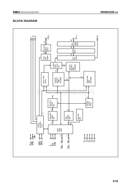
FUNCTIONAL DESCRIPTION
Instruction Register (IR) and Data Register (DR)
These two registers are selected by the REGISTER SELECTOR (RS) pin.
The DR is selected when the "H" level is input to the RS pin and IR is selected when the "L"
level is input.
The IR is used to store the address of the display data RAM (DD RAM) or character
generator RAM (CG RAM) and instruction code.
The IR can be written, but not be read by the microcomputer (CPU).
The DR is used to write and read the data to and from the DD RAM or CG RAM.
The data written to DR by the CPU is automatically written to the DD RAM or CG RAM
as an internal operation.
When an address code is written to IR, the data (of the specified address) is automatically
transferred from the DD RAM or CG RAM to the DR. Next, when the CPU reads the DR,
it is possible to verify DD RAM or CG RAM data from the DR data.
After the writing of DR by the CPU, the next adress in the DD RAM or CG RAM is selected
to be ready for the next CPU writing.
Likewise, after the reading out of DR by the CPU, DD RAM or CG RAM data is read out
by the DR to be ready for the next CPU reading.
Write/read to and from both registers is carried out by the READ/WRITE (R/W) pin.
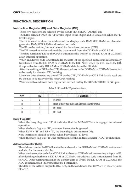
Table 1 RS and R/W pins functions
R/W
L
H
L
H
RS
L
L
H
H
IR write
Function
Read of busy flag (BF) and address counter (ADC)
DR write
DR read
Busy Flag (BF)
When the busy flag is at "H", it indicates that the MSM6222B-xx is engaged in internal
operation.
When the busy flag is at "H", any new instruction is ignored.
When R/W = "H" and RS = "L", the busy flag is output from DB
7
.
New instruction should be input when busy flag is "L" level.
When the busy flag is at "H", the output code of the address counter (ADC) is undefined.
Address Counter (ADC)
The address counter (ADC) allocates the address for the DD RAM and CG RAM write/read
and also for the cursor display.
When the instruction code for a DD RAM address or CG RAM address setting is input to IR,
after deciding whether it is DD RAM or CG RAM, the address code is transferred from IR
to ADC. After writing (reading) the display data to (from) the DD RAM or CG RAM, the
ADC is incremented (decremented) by 1 internally.
The data of the ADC is output to DB
0
- DB
6
on the conditions that R/W = "H", RS = "L", and
BF = "L".
13/45


 1
1
 2
2
 3
3
 4
4
 5
5
 6
6
 7
7
 8
8
 9
9
 10
10
 11
11
 12
12
 13
13
 14
14
 15
15
 16
16
 17
17
 18
18
 19
19
 20
20
 21
21
 22
22
 23
23
 24
24
 25
25
 26
26
 27
27
 28
28
 29
29
 30
30
 31
31
 32
32
 33
33
 34
34
 35
35
 36
36
 37
37
 38
38
 39
39
 40
40
 41
41
 42
42
 43
43
 44
44
 45
45
