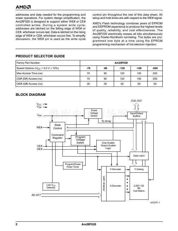
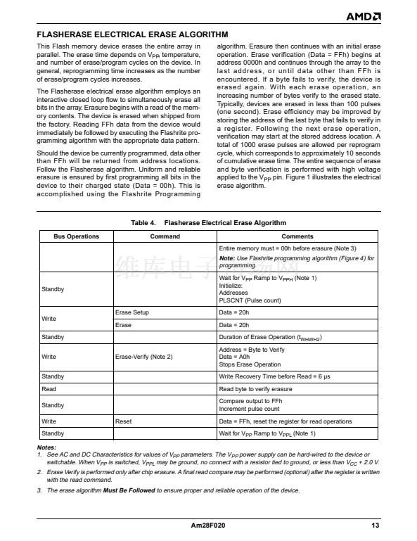
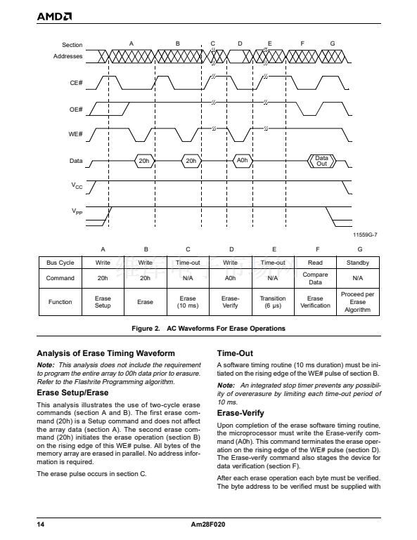
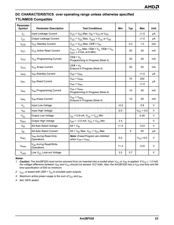
ERASE, PROGRAM, AND READ MODE
When V
PP
is equal to 12.0 V 卤 5%, the command reg-
ister is active. All functions are available. That is, the
device can program, erase, read array or autoselect
data, or be standby mode.
Refer to AC Write Characteristics and the Erase/Pro-
gramming Waveforms for specific timing parameters.
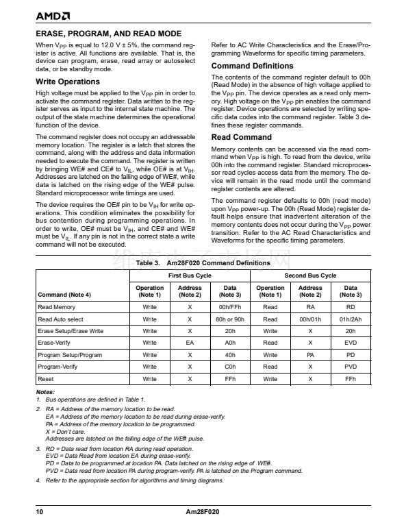
Command Definitions
The contents of the command register default to 00h
(Read Mode) in the absence of high voltage applied to
the V
PP
pin. The device operates as a read only mem-
ory. High voltage on the V
PP
pin enables the command
register. Device operations are selected by writing spe-
cific data codes into the command register. Table 3 de-
fines these register commands.
Write Operations
High voltage must be applied to the V
PP
pin in order to
activate the command register. Data written to the reg-
ister serves as input to the internal state machine. The
output of the state machine determines the operational
function of the device.
The command register does not occupy an addressable
memory location. The register is a latch that stores the
command, along with the address and data information
needed to execute the command. The register is written
by bringing WE# and CE# to V
IL
, while OE# is at V
IH
.
Addresses are latched on the falling edge of WE#, while
data is latched on the rising edge of the WE# pulse.
Standard microprocessor write timings are used.
The device requires the OE# pin to be V
IH
for write op-
erations. This condition eliminates the possibility for
bus contention during programming operations. In
order to write, OE# must be V
IH
, and CE# and WE#
must be V
IL
. If any pin is not in the correct state a write
command will not be executed.
Table 3.
Read Command
Memory contents can be accessed via the read com-
mand when V
PP
is high. To read from the device, write
00h into the command register. Standard microproces-
sor read cycles access data from the memory. The de-
vice will remain in the read mode until the command
register contents are altered.
The command register defaults to 00h (read mode)
upon V
PP
power-up. The 00h (Read Mode) register de-
fault helps ensure that inadvertent alteration of the
memory contents does not occur during the V
PP
power
transition. Refer to the AC Read Characteristics and
Waveforms for the specific timing parameters.
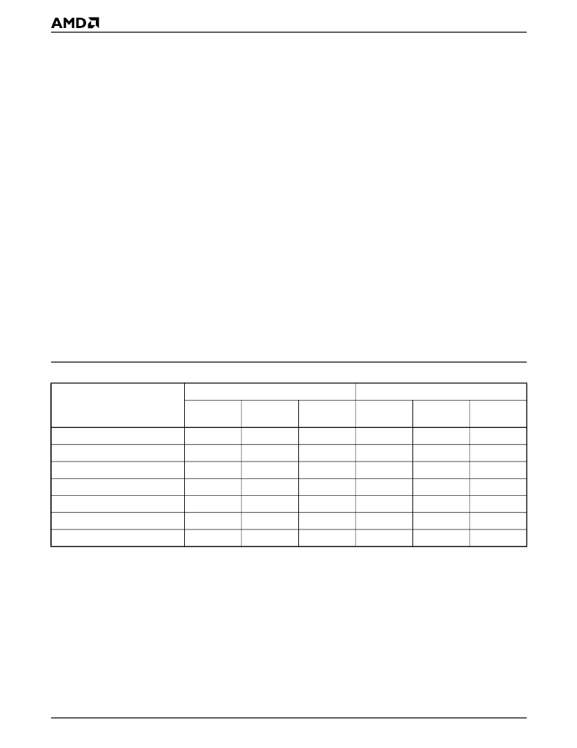
Am28F020 Command Definitions
First Bus Cycle
Second Bus Cycle
Data
(Note 3)
00h/FFh
80h or 90h
20h
A0h
40h
C0h
FFh
Operation
(Note 1)
Read
Read
Write
Read
Write
Read
Write
Address
(Note 2)
RA
00h/01h
X
X
PA
X
X
Data
(Note 3)
RD
01h/2Ah
20h
EVD
PD
PVD
FFh
Command (Note 4)
Read Memory
Read Auto select
Erase Setup/Erase Write
Erase-Verify
Program Setup/Program
Program-Verify
Reset
Operation
(Note 1)
Write
Write
Write
Write
Write
Write
Write
Address
(Note 2)
X
X
X
EA
X
X
X
Notes:
1. Bus operations are defined in Table 1.
2. RA = Address of the memory location to be read.
EA = Address of the memory location to be read during erase-verify.
PA = Address of the memory location to be programmed.
X = Don鈥檛 care.
Addresses are latched on the falling edge of the WE
#
pulse.
3. RD = Data read from location RA during read operation.
EVD = Data Read from location EA during erase-verify.
PD = Data to be programmed at location PA. Data latched on the rising edge of WE
#
.
PVD = Data read from location PA during program-verify. PA is latched on the Program command.
4. Refer to the appropriate section for algorithms and timing diagrams.
10
Am28F020


 1
1
 2
2
 3
3
 4
4
 5
5
 6
6
 7
7
 8
8
 9
9
 10
10
 11
11
 12
12
 13
13
 14
14
 15
15
 16
16
 17
17
 18
18
 19
19
 20
20
 21
21
 22
22
 23
23
 24
24
 25
25
 26
26
 27
27
 28
28
 29
29
 30
30
 31
31
 32
32
 33
33
 34
34
 35
35
