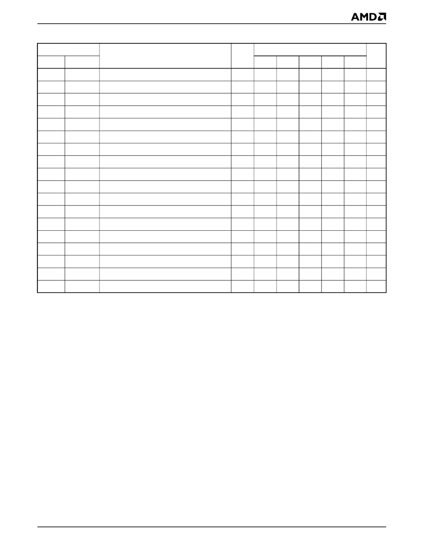
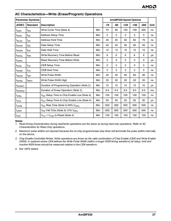
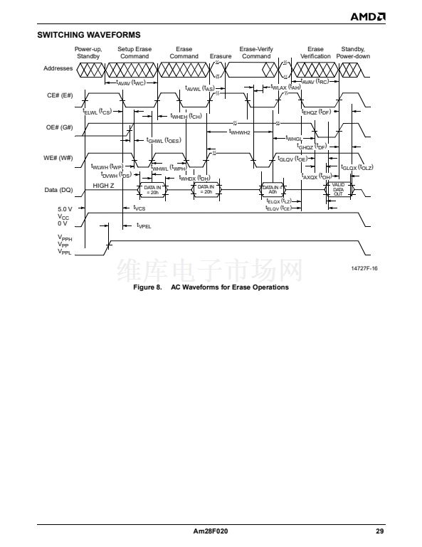
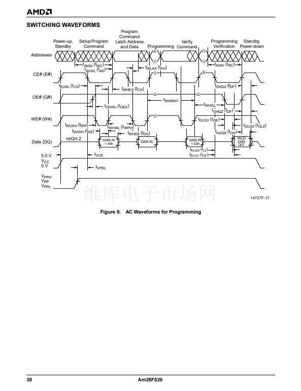
AC Characteristics鈥擶rite (Erase/Program) Operations
Parameter Symbols
JEDEC
t
AVAV
t
AVWL
t
WLAX
t
DVWH
t
WHDX
t
WHGL
t
GHWL
t
ELWL
t
WHEH
t
WLWH
t
WHWL
t
WHWH1
t
WHWH2
t
VPEL
t
VCS
t
VPPR
t
VPPF
t
LKO
t
CS
t
CH
t
WP
t
WPH
Standard
t
WC
t
AS
t
AH
t
DS
t
DH
t
WR
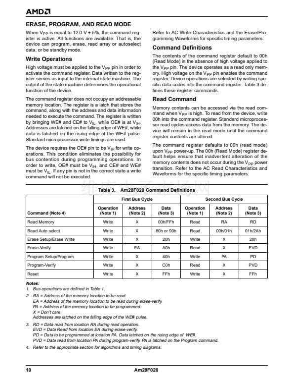
Description
Write Cycle Time (Note 4)
Address Setup Time
Address Hold Time
Data Setup Time
Data Hold Time
Write Recovery Time Before Read
Read Recovery Time Before Write
CE
#
Setup Time
CE
#
Hold Time
Write Pulse Width
Write Pulse Width High
Duration of Programming Operation (Note 2)
Duration of Erase Operation (Note 2)
V
PP
Setup Time to Chip Enable Low (Note 4)
V
CC
Setup Time to Chip Enable Low (Note 4)
V
PP
Rise Time (Note 4) 90% V
PPH
V
PP
Fall Time (Note 4) 10% V
PPL
V
CC
< V
LKO
to Reset (Note 4)
Min
Min
Min
Min
Min
Min
Min
Min
Min
Min
Min
Min
Min
Min
Min
Min
Min
Min
-70
70
0
45
45
10
6
0
0
0
45
20
10
9.5
100
50
500
500
100
Am28F020 Speed Options
-90
90
0
45
45
10
6
0
0
0
45
20
10
9.5
100
50
500
500
100
-120
120
0
50
50
10
6
0
0
0
50
20
10
9.5
100
50
500
500
100
-150
150
0
60
50
10
6
0
0
0
60
20
10
9.5
100
50
500
500
100
-200
200
0
75
50
10
6
0
0
0
60
20
10
9.5
100
50
500
500
100
Unit
ns
ns
ns
ns
ns
碌s
碌s
ns
ns
ns
ns
碌s
ms
ns
碌s
ns
ns
ns
Notes:
1. Read timing characteristics during read/write operations are the same as during read-only operations. Refer to AC
Characteristics for Read Only operations.
2. Maximum pulse widths not required because the on-chip program/erase stop timer will terminate the pulse widths internally
on the device.
3. Chip Enable-Controlled Writes: Write operations are driven by the valid combination of Chip Enable (CE#) and Write Enable
(WE#). In systems where CE# defines the Write Pulse Width (within a longer WE# timing waveform) all setup, hold and
inactive WE# times should be measured relative to the CE# waveform.
4. Not 100% tested.
Am28F020
27


 1
1
 2
2
 3
3
 4
4
 5
5
 6
6
 7
7
 8
8
 9
9
 10
10
 11
11
 12
12
 13
13
 14
14
 15
15
 16
16
 17
17
 18
18
 19
19
 20
20
 21
21
 22
22
 23
23
 24
24
 25
25
 26
26
 27
27
 28
28
 29
29
 30
30
 31
31
 32
32
 33
33
 34
34
 35
35
