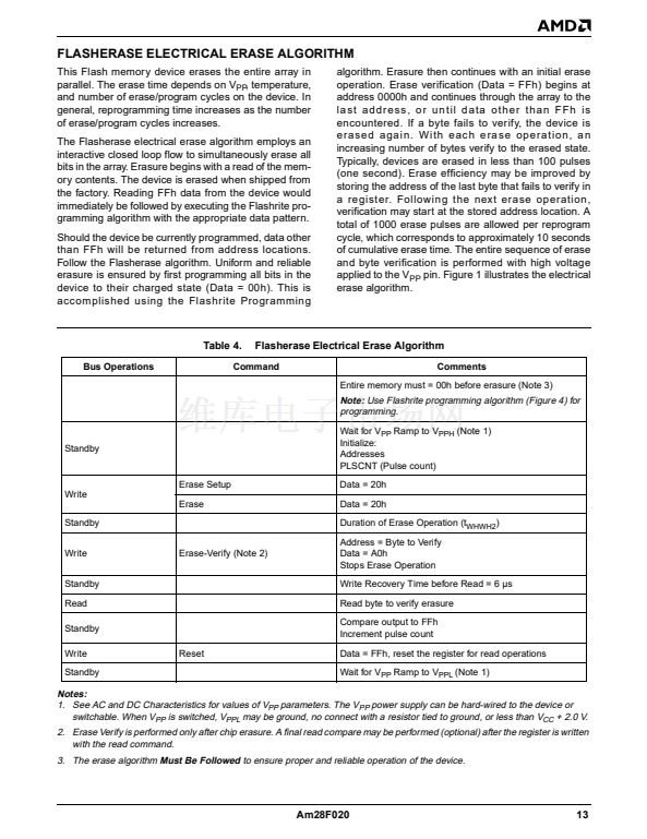
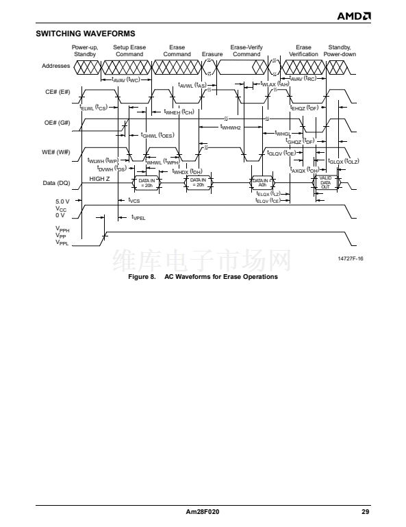
FLASHERASE ERASE SEQUENCE
Erase Setup
Erase Setup is the first of a two-cycle erase command.
It is a command-only operation that stages the device
for bulk chip erase. The array contents are not altered
with this command. 20h is written to the command reg-
ister in order to perform the Erase Setup operation.
ated by writing A0h to the register. The byte address to
be verified must be supplied with the command. Ad-
dresses are latched on the falling edge of the WE#
pulse or CE# pulse, whichever occurs later. The rising
edge of the WE# pulse terminates the erase operation.
Margin Verify
During the Erase-verify operation, the device applies
an i nter nally generated margin vol tage to the
addressed byte. Reading FFh from the addressed byte
indicates that all bits in the byte are properly erased.
Erase
The second two-cycle erase command initiates the
bulk erase operation. You must write the Erase com-
mand (20h) again to the register. The erase operation
begins with the rising edge of the WE# pulse. The
erase operation must be terminated by writing a new
command (Erase-verify) to the register.
This two step sequence of the Setup and Erase com-
mands helps to ensure that memory contents are not
accidentally erased. Also, chip erasure can only occur
when high voltage is applied to the V
PP
pin and all con-
trol pins are in their proper state. In absence of this high
voltage, memory contents cannot be altered. Refer to
AC Erase Characteristics and Waveforms for specific
timing parameters.
Verify Next Address
You must write the Erase-verify command with the ap-
propriate address to the register prior to verification of
each address. Each new address is latched on the fall-
ing edge of WE# or CE# pulse, whichever occurs later.
The process continues for each byte in the memory
array until a byte does not return FFh data or all the
bytes in the array are accessed and verified.
If an address is not verified to FFh data, the entire chip
is erased again (refer to Erase Setup/Erase). Erase
verification then resumes at the address that failed to
verify. Erase is complete when all bytes in the array
have been verified. The device is now ready to be pro-
grammed. At this point, the verification operation is ter-
minated by writing a valid command (e.g. Program
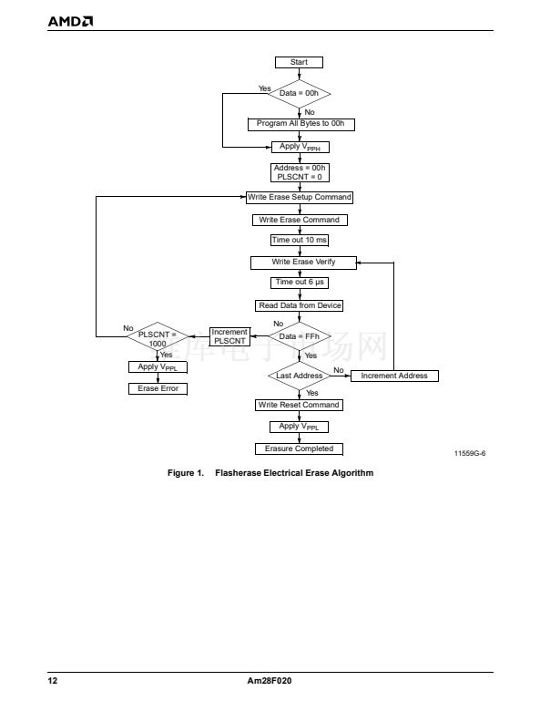
Setup) to the command register. Figure 1 and Table 4,
the Flasherase electrical erase algorithm, illustrate how
commands and bus operations are combined to per-
form electrical erasure. Refer to AC Erase Characteris-
tics and Waveforms for specific timing parameters.
Note:
The Flash memory device must be fully
programmed to 00h data prior to erasure. This
equalizes the charge on all memory cells ensuring
reliable erasure.
Erase-Verify Command
The erase operation erases all bytes of the array
in parallel. After the erase operation, all bytes must be
sequentially verified. The Erase-verify operation is initi-
Am28F020
11


 1
1
 2
2
 3
3
 4
4
 5
5
 6
6
 7
7
 8
8
 9
9
 10
10
 11
11
 12
12
 13
13
 14
14
 15
15
 16
16
 17
17
 18
18
 19
19
 20
20
 21
21
 22
22
 23
23
 24
24
 25
25
 26
26
 27
27
 28
28
 29
29
 30
30
 31
31
 32
32
 33
33
 34
34
 35
35
