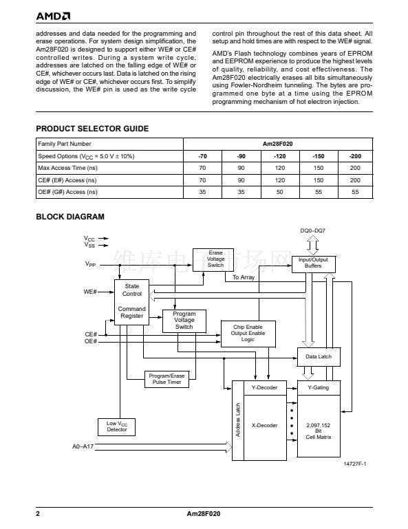
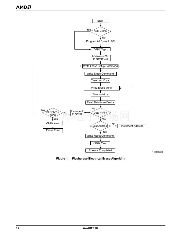
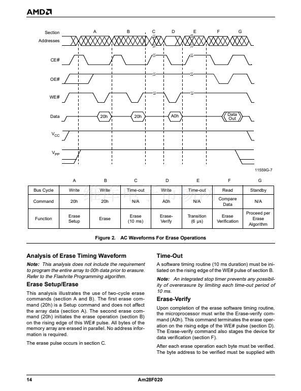
FLASHERASE ELECTRICAL ERASE ALGORITHM
This Flash memory device erases the entire array in
parallel. The erase time depends on V
PP
, temperature,
and number of erase/program cycles on the device. In
general, reprogramming time increases as the number
of erase/program cycles increases.
The Flasherase electrical erase algorithm employs an
interactive closed loop flow to simultaneously erase all
bits in the array. Erasure begins with a read of the mem-
ory contents. The device is erased when shipped from
the factory. Reading FFh data from the device would
immediately be followed by executing the Flashrite pro-
gramming algorithm with the appropriate data pattern.
Should the device be currently programmed, data other
than FFh will be returned from address locations.
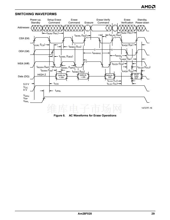
Follow the Flasherase algorithm. Uniform and reliable
erasure is ensured by first programming all bits in the
device to their charged state (Data = 00h). This is
accomplished using the Flashrite Programming
algorithm. Erasure then continues with an initial erase
operation. Erase verification (Data = FFh) begins at
address 0000h and continues through the array to the
l a s t a dd re s s , o r u n ti l d ata o th er th an FF h i s
encountered. If a byte fails to verify, the device is
erase d agai n. W i th eac h e ra s e operati on , a n
increasing number of bytes verify to the erased state.
Typically, devices are erased in less than 100 pulses
(one second). Erase efficiency may be improved by
storing the address of the last byte that fails to verify in
a register. Following the nex t erase operation,
verification may start at the stored address location. A
total of 1000 erase pulses are allowed per reprogram
cycle, which corresponds to approximately 10 seconds
of cumulative erase time. The entire sequence of erase
and byte verification is performed with high voltage
applied to the V
PP
pin. Figure 1 illustrates the electrical
erase algorithm.
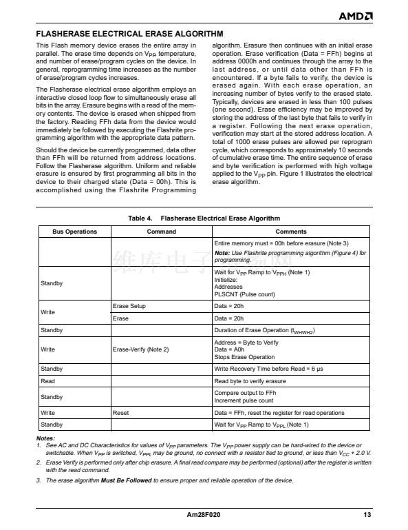
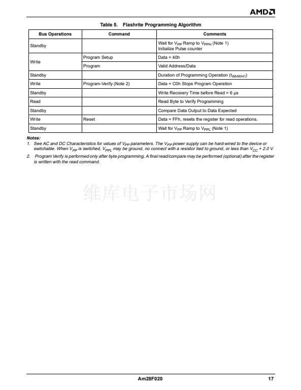
Table 4.
Bus Operations
Flasherase Electrical Erase Algorithm
Comments
Entire memory must = 00h before erasure (Note 3)
Command
Note:
Use Flashrite programming algorithm (Figure 4) for
programming.
Wait for V
PP
Ramp to V
PPH
(Note 1)
Initialize:
Addresses
PLSCNT (Pulse count)
Erase Setup
Write
Erase
Standby
Write
Standby
Read
Standby
Write
Standby
Reset
Erase-Verify (Note 2)
Data = 20h
Duration of Erase Operation (t
WHWH2
)
Address = Byte to Verify
Data = A0h
Stops Erase Operation
Write Recovery Time before Read = 6 碌s
Read byte to verify erasure
Compare output to FFh
Increment pulse count
Data = FFh, reset the register for read operations
Wait for V
PP
Ramp to V
PPL
(Note 1)
Data = 20h
Standby
Notes:
1. See AC and DC Characteristics for values of V
PP
parameters. The V
PP
power supply can be hard-wired to the device or
switchable. When V
PP
is switched, V
PPL
may be ground, no connect with a resistor tied to ground, or less than V
CC
+ 2.0 V.
2. Erase Verify is performed only after chip erasure. A final read compare may be performed (optional) after the register is written
with the read command.
3. The erase algorithm
Must Be Followed
to ensure proper and reliable operation of the device.
Am28F020
13


 1
1
 2
2
 3
3
 4
4
 5
5
 6
6
 7
7
 8
8
 9
9
 10
10
 11
11
 12
12
 13
13
 14
14
 15
15
 16
16
 17
17
 18
18
 19
19
 20
20
 21
21
 22
22
 23
23
 24
24
 25
25
 26
26
 27
27
 28
28
 29
29
 30
30
 31
31
 32
32
 33
33
 34
34
 35
35
