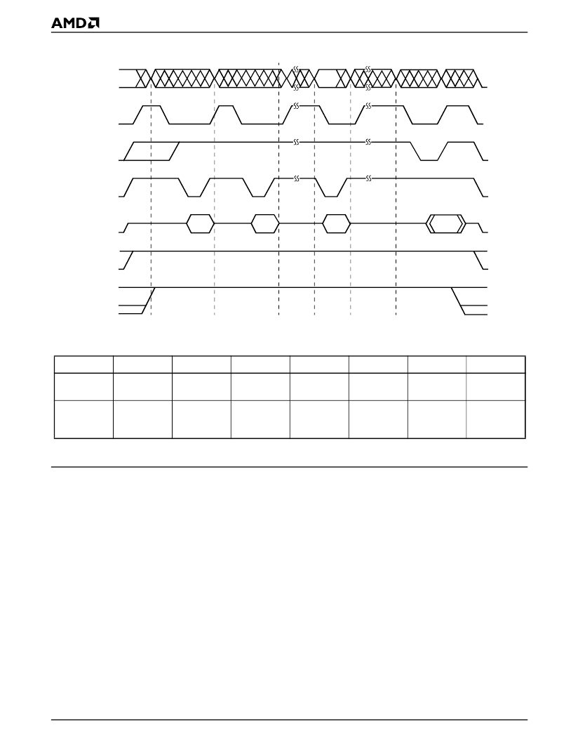
Section
Addresses
A
B
C
D
E
F
G
CE
#
OE
#
WE
#
Data
20h
20h
A0h
Data
Out
V
CC
V
PP
11559G-7
A
Bus Cycle
Command
Write
20h
Erase
Setup
B
Write
20h
C
Time-out
N/A
Erase
(10 ms)
D
Write
A0h
Erase-
Verify
E
Time-out
N/A
Transition
(6 碌s)
F
Read
Compare
Data
Erase
Verification
G
Standby
N/A
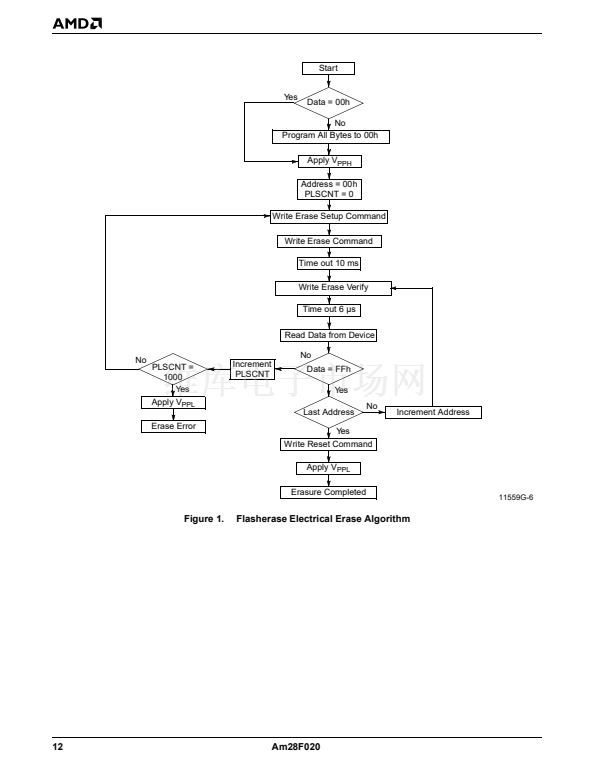
Proceed per
Erase
Algorithm
Function
Erase
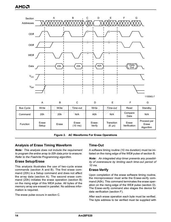
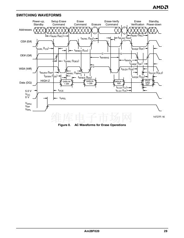
Figure 2. AC Waveforms For Erase Operations
Analysis of Erase Timing Waveform
Note:
This analysis does not include the requirement
to program the entire array to 00h data prior to erasure.
Refer to the Flashrite Programming algorithm.
Time-Out
A software timing routine (10 ms duration) must be ini-
tiated on the rising edge of the WE# pulse of section B.
Erase Setup/Erase
This analysis illustrates the use of two-cycle erase
commands (section A and B). The first erase com-
mand (20h) is a Setup command and does not affect
the array data (section A). The second erase com-
mand (20h) initiates the erase operation (section B)
on the rising edge of this WE# pulse. All bytes of the
memory array are erased in parallel. No address infor-
mation is required.
The erase pulse occurs in section C.
Note:
An integrated stop timer prevents any possibil-
ity of overerasure by limiting each time-out period of
10 ms.
Erase-Verify
Upon completion of the erase software timing routine,
the microprocessor must write the Erase-verify com-
mand (A0h). This command terminates the erase oper-
ation on the rising edge of the WE# pulse (section D).
The Erase-verify command also stages the device for
data verification (section F).
After each erase operation each byte must be verified.
The byte address to be verified must be supplied with
14
Am28F020


 1
1
 2
2
 3
3
 4
4
 5
5
 6
6
 7
7
 8
8
 9
9
 10
10
 11
11
 12
12
 13
13
 14
14
 15
15
 16
16
 17
17
 18
18
 19
19
 20
20
 21
21
 22
22
 23
23
 24
24
 25
25
 26
26
 27
27
 28
28
 29
29
 30
30
 31
31
 32
32
 33
33
 34
34
 35
35
