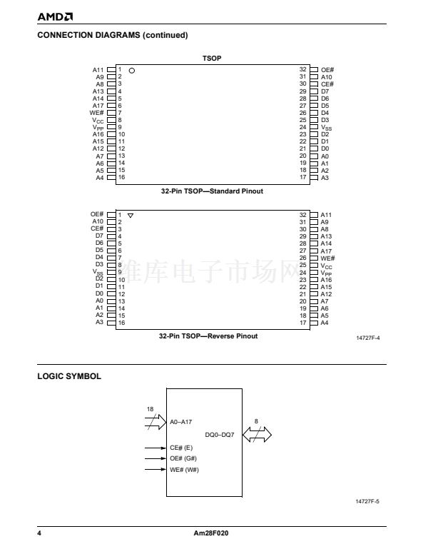
addresses and data needed for the programming and
erase operations. For system design simplification, the
Am28F020 is designed to support either WE# or CE#
controlled w rites. During a system write cycle,
addresses are latched on the falling edge of WE# or
CE#, whichever occurs last. Data is latched on the rising
edge of WE# or CE#, whichever occurs first. To simplify
discussion, the WE# pin is used as the write cycle
control pin throughout the rest of this data sheet. All
setup and hold times are with respect to the WE# signal.
AMD鈥檚 Flash technology combines years of EPROM
and EEPROM experience to produce the highest levels
of quality, reliability, and cost effectiveness. The
Am28F020 electrically erases all bits simultaneously
using Fowler-Nordheim tunneling. The bytes are pro-
grammed one byte at a time using the EPROM
programming mechanism of hot electron injection.
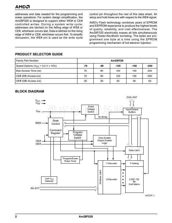
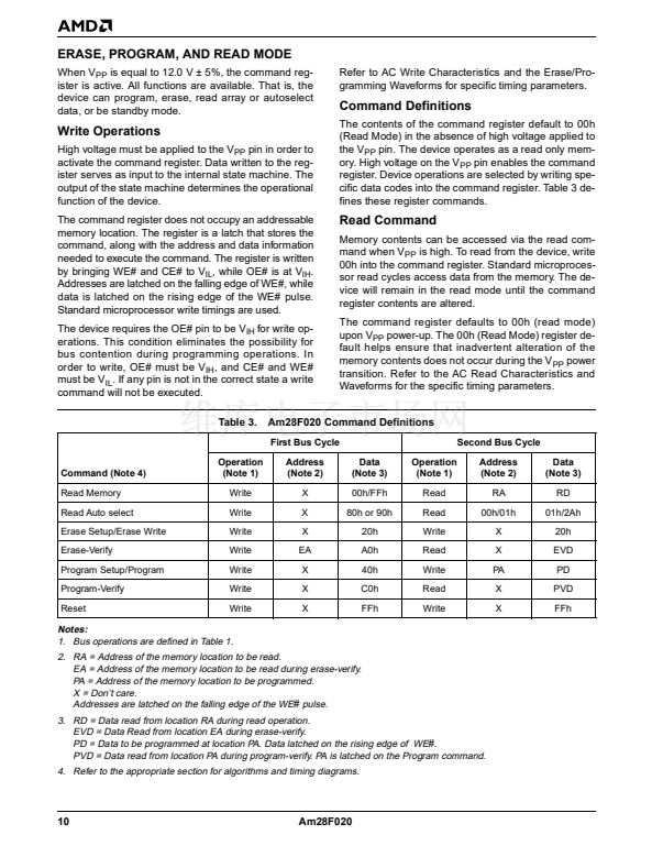
PRODUCT SELECTOR GUIDE
Family Part Number
Speed Options (V
CC
= 5.0 V
卤
10%)
Max Access Time (ns)
CE
#
(E
#
) Access (ns)
OE
#
(G
#
) Access (ns)
-70
70
70
35
-90
90
90
35
Am28F020
-120
120
120
50
-150
150
150
55
-200
200
200
55
BLOCK DIAGRAM
DQ0鈥揇Q7
V
CC
V
SS
V
PP
Erase
Voltage
Switch
Input/Output
Buffers
To Array
WE#
State
Control
Command
Register
CE#
OE#
Program
Voltage
Switch
Chip Enable
Output Enable
Logic
Data Latch
Program/Erase
Pulse Timer
Y-Decoder
Address Latch
Y-Gating
Low V
CC
Detector
X-Decoder
2,097,152
Bit
Cell Matrix
A0鈥揂17
14727F-1
2
Am28F020


 1
1
 2
2
 3
3
 4
4
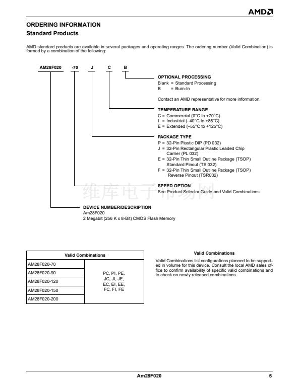 5
5
 6
6
 7
7
 8
8
 9
9
 10
10
 11
11
 12
12
 13
13
 14
14
 15
15
 16
16
 17
17
 18
18
 19
19
 20
20
 21
21
 22
22
 23
23
 24
24
 25
25
 26
26
 27
27
 28
28
 29
29
 30
30
 31
31
 32
32
 33
33
 34
34
 35
35
