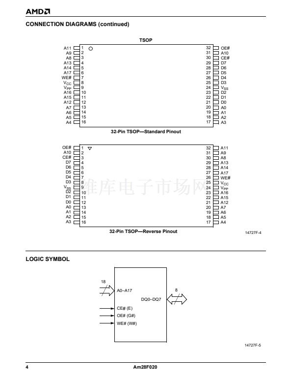
PIN DESCRIPTION
A0鈥揂17
Address Inputs for memory locations. Internal latches
hold addresses during write cycles.
V
CC
Power supply for device operation. (5.0 V
卤
5% or 10%)
CE
#
(E
#
)
Chip Enable active low input activates the chip鈥檚 control
logic and input buffers. Chip Enable high will deselect
the device and operates the chip in stand-by mode.
V
PP
Program voltage input. V
PP
must be at high voltage in
order to write to the command register. The command
register controls all functions required to alter the
memory array contents. Memory contents cannot be
altered when V
PP
鈮?/div>
V
CC
+2 V.
DQ0鈥揇Q7
Data Inputs during memory write cycles. Internal
latches hold data during write cycles. Data Outputs
during memory read cycles.
V
SS
Ground
WE
#
(W
#
)
Write Enable active low input controls the write function
of the command register to the memory array. The
target address is latched on the falling edge of the
Write Enable pulse and the appropriate data is latched
on the rising edge of the pulse. Write Enable high
inhibits writing to the device.
NC
No Connect-corresponding pin is not connected
internally to the die.
OE
#
(G
#
)
Output Enable active low input gates the outputs of the
device through the data buffers during memory read
cycles. Output Enable is high during command
sequencing and program/erase operations.
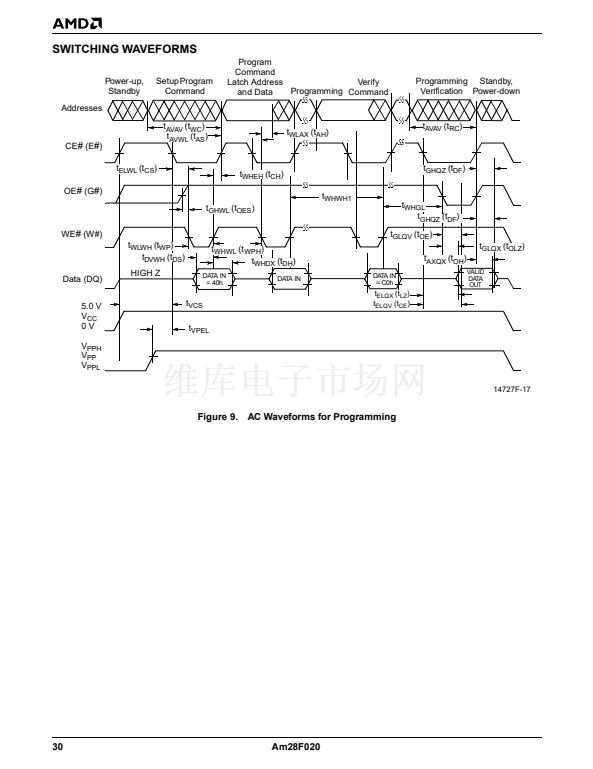
6
Am28F020


 1
1
 2
2
 3
3
 4
4
 5
5
 6
6
 7
7
 8
8
 9
9
 10
10
 11
11
 12
12
 13
13
 14
14
 15
15
 16
16
 17
17
 18
18
 19
19
 20
20
 21
21
 22
22
 23
23
 24
24
 25
25
 26
26
 27
27
 28
28
 29
29
 30
30
 31
31
 32
32
 33
33
 34
34
 35
35
