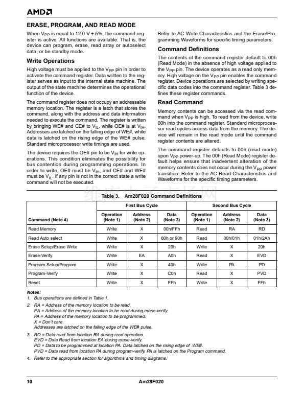
BASIC PRINCIPLES
The device uses 100% TTL-level control inputs to
manage the command register. Erase and repro-
gramming operations use a fixed 12.0 V
卤
5% high
voltage input.
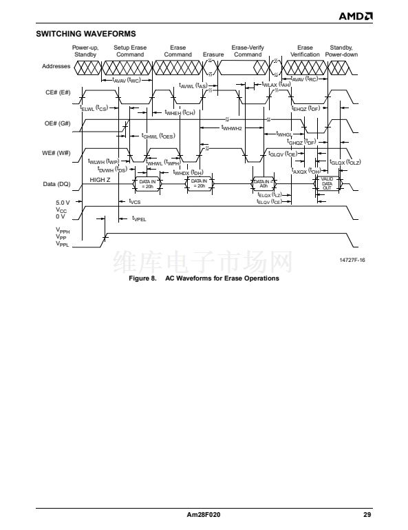
formation must be supplied with the Erase-verify
command. This command verifies the margin and
outputs the addressed byte in order to compare the
array data with FFh data (Byte erased).
After successful data verification the Erase-verify
command is written again with new address infor-
mation. Each byte of the array is sequentially veri-
fied in this manner.
If data of the addressed location is not verified, the
Erase sequence is repeated until the entire array is
successfully verified or the sequence is repeated
1000 times.
Flashrite Programming Sequence
A three step command sequence (a two-cycle Program
command and one cycle Verify command) is required
to program a byte of the Flash array. Refer to the Flash-
rite Algorithm.
1.
Program Setup:
Write the Setup Program com-
mand to the command register.
2.
Program:
Write the Program command to the com-
mand register with the appropriate Address and
Data. The system software routines must now time-
out the program pulse width (10 碌s) prior to issuing
the Program-verify command. An integrated stop
timer prevents any possibility of overprogramming.
3.
Program-Verify:
Write the Program-verify com-
mand to the command register. This command ter-
minates the programming operation. In addition,
this command verifies the margin and outputs the
byte just programmed in order to compare the array
data with the original data programmed. After suc-
cessful data verification, the programming se-
quence is initiated again for the next byte address to
be programmed.
If data is not verified successfully, the Program se-
quence is repeated until a successful comparison is
verified or the sequence is repeated 25 times.
Read Only Memory
Without high V
PP
voltage, the device functions as a
read only memory and operates like a standard
EPROM. The control inputs still manage traditional
read, standby, output disable, and Auto select modes.
Command Register
The command register is enabled only when high volt-
age is applied to the V
PP
pin. The erase and repro-
gramming operations are only accessed via the
register. In addition, two-cycle commands are required
for erase and reprogramming operations. The tradi-
tional read, standby, output disable, and Auto select
modes are available via the register.
The device鈥檚 command register is written using stan-
dard microprocessor write timings. The register con-
trols an internal state machine that manages all device
operations. For system design simplification, the de-
vice is designed to support either WE# or CE# con-
trolled writes. During a system write cycle, addresses
are latched on the falling edge of WE# or CE# which-
ever occurs last. Data is latched on the rising edge of
WE# or CE# whichever occur first. To simplify the fol-
lowing discussion, the WE# pin is used as the write
cycle control pin throughout the rest of this text. All
setup and hold times are with respect to the WE# sig-
nal.
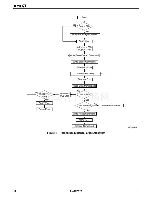
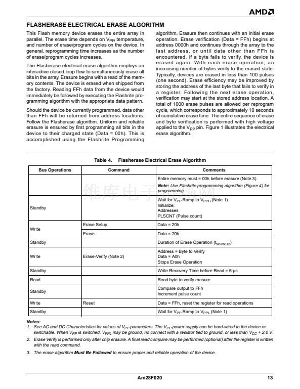
Overview of Erase/Program Operations
Flasherase鈩?Sequence
A multiple step command sequence is required to
erase the Flash device (a two-cycle Erase command
and repeated one cycle verify commands).
Note:
The Flash memory array must be completely
programmed to 0鈥檚 prior to erasure. Refer to the
Flashrite鈩?Programming Algorithm.
1.
Erase Setup:
Write the Setup Erase command to
the command register.
2.
Erase:
Write the Erase command (same as Setup
Erase command) to the command register again.
The second command initiates the erase operation.
The system software routines must now time-out
the erase pulse width (10 ms) prior to issuing the
Erase-verify command. An integrated stop timer
prevents any possibility of overerasure.
3.
Erase-Verify:
Write the Erase-verify command to
the command register. This command terminates
the erase operation. After the erase operation,
each byte of the array must be verified. Address in-
Data Protection
The device is designed to offer protection against acci-
dental erasure or programming caused by spurious
system level signals that may exist during power transi-
tions. The device powers up in its read only state. Also,
with its control register architecture, alteration of the
memory contents only occurs after successful comple-
tion of specific command sequences.
The device also incorporates several features to pre-
vent inadvertent write cycles resulting fromV
CC
power-
up and power-down transitions or system noise.
Low V
CC
Write Inhibit
To avoid initiation of a write cycle during V
CC
power-up
and power-down, the device locks out write cycles for
Am28F020
7


 1
1
 2
2
 3
3
 4
4
 5
5
 6
6
 7
7
 8
8
 9
9
 10
10
 11
11
 12
12
 13
13
 14
14
 15
15
 16
16
 17
17
 18
18
 19
19
 20
20
 21
21
 22
22
 23
23
 24
24
 25
25
 26
26
 27
27
 28
28
 29
29
 30
30
 31
31
 32
32
 33
33
 34
34
 35
35
