V
CC
< V
LKO
(see DC Characteristics section for
voltages). When V
CC
< V
LKO
, the command register is
disabled, all internal program/erase circuits are
disabled, and the device resets to the read mode. The
device ignores all writes until V
CC
> V
LKO
. The user
must ensure that the control pins are in the correct logic
state when V
CC
> V
LKO
to prevent uninitentional writes.
Logical Inhibit
Writing is inhibited by holding any one of OE# = V
IL
, CE#
= V
IH
or WE# = V
IH
. To initiate a write cycle CE# and
WE# must be a logical zero while OE# is a logical one.
Power-Up Write Inhibit
Power-up of the device with WE# = CE# = V
IL
and
OE# = V
IH
will not accept commands on the rising
edge of WE#. The internal state machine is automat-
ically reset to the read mode on power-up.
Write Pulse 鈥淕litch鈥?Protection
Noise pulses of less than 10 ns (typical) on OE#, CE#
or WE# will not initiate a write cycle.
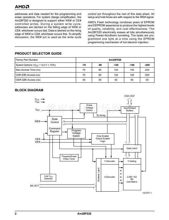
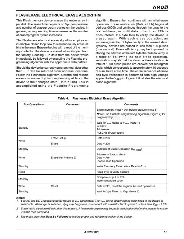
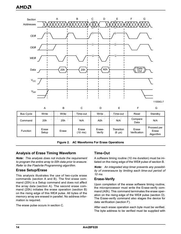
FUNCTIONAL DESCRIPTION
Description of User Modes
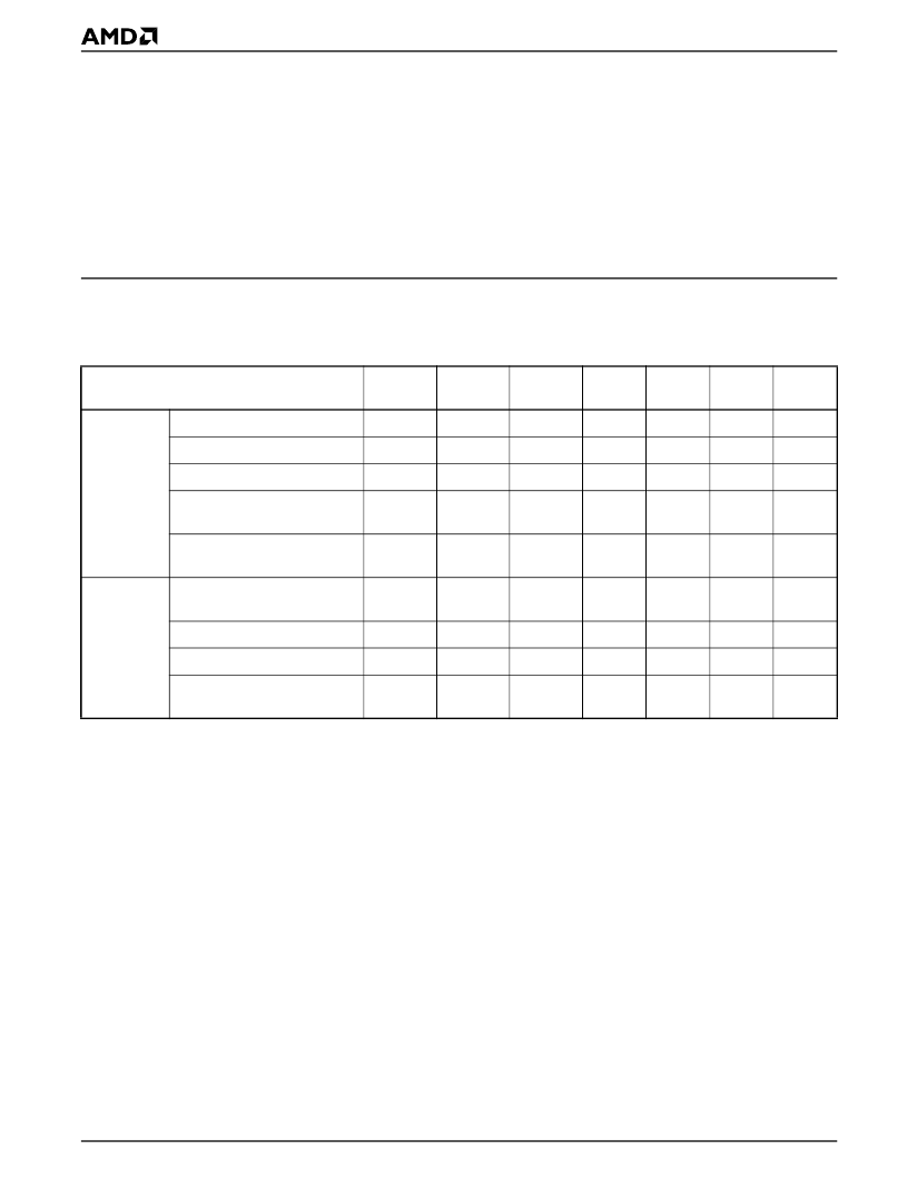
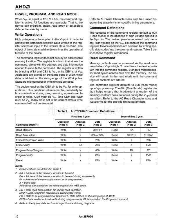
Table 1.
Operation
Read
Standby
Output Disable
Read-Only
Auto-Select Manufacturer
Code (Note 2)
Auto-Select Device Code
(Note 2)
Read
Standby (Note 5)
Read/Write
Output Disable
Write
Am28F020 Device Bus Operations
CE
#
(E
#
)
V
IL
V
IH
V
IL
V
IL
V
IL
V
IL
V
IH
V
IL
V
IL
V
PP
OE
#
(G
#
) WE
#
(W
#
) (Note 1)
V
IL
X
V
IH
V
IL
V
IL
V
IL
X
V
IH
V
IH
X
X
V
IH
V
IH
V
IH
V
IH
X
V
IH
V
IL
V
PPL
V
PPL
V
PPL
V
PPL
V
PPL
V
PPH
V
PPH
V
PPH
V
PPH
A0
A0
X
X
V
IL
V
IH
A0
X
X
A0
A9
A9
X
X
V
ID
(Note 3)
V
ID
(Note 3)
A9
X
X
A9
I/O
D
OUT
HIGH Z
HIGH Z
CODE
(01h)
CODE
(2Ah)
D
OUT
(Note 4)
HIGH Z
HIGH Z
D
IN
(Note 6)
Legend:
X = Don鈥檛 care, where Don鈥檛 Care is either V
IL
or V
IH
levels. V
PPL
= V
PP
鈮?/div>
V
CC
+ 2 V. See DC Characteristics for voltage levels
of V
PPH
. 0 V < An < V
CC
+ 2 V, (normal TTL or CMOS input levels, where n = 0 or 9).
Notes:
1. V
PPL
may be grounded, connected with a resistor to ground, or < V
CC
+ 2.0 V. V
PPH
is the programming voltage specified for
the device. Refer to the DC characteristics. When V
PP
= V
PPL
, memory contents can be read but not written or erased.
2. Manufacturer and device codes may also be accessed via a command register write sequence. Refer to Table 2.
3. 11.5 < V
ID
< 13.0 V. Minimum V
ID
rise time and fall time (between 0 and V
ID
voltages) is 500 ns.
4. Read operation with V
PP
= V
PPH
may access array data or the Auto select codes.
5. With V
PP
at high voltage, the standby current is I
CC
+ I
PP
(standby).
6. Refer to Table 3 for valid D
IN
during a write operation.
7. All inputs are Don鈥檛 Care unless otherwise stated, where Don鈥檛 Care is either V
IL
or V
IH
levels. In the Auto select mode all
addresses except A9 and A0 must be held at V
IL
.
8. If V
CC
鈮?/div>
1.0 Volt, the voltage difference between V
PP
and V
CC
should not exceed 10.0 volts. Also, the Am28F010 has a V
PP
rise time and fall time specification of 500 ns minimum.
8
Am28F020


 1
1
 2
2
 3
3
 4
4
 5
5
 6
6
 7
7
 8
8
 9
9
 10
10
 11
11
 12
12
 13
13
 14
14
 15
15
 16
16
 17
17
 18
18
 19
19
 20
20
 21
21
 22
22
 23
23
 24
24
 25
25
 26
26
 27
27
 28
28
 29
29
 30
30
 31
31
 32
32
 33
33
 34
34
 35
35
